Fundamental guide to understanding DRAM performance and timing parameters
How DRAM timing parameters affect HBM, LPDDR, GDDR bandwidth. How to get the most performance out of your memory.
In my last post, I stated that in order to design a robust memory subsystem, you must understand 3 key dimensions of the DRAM:
PhysicalStructure- We tackled this last time, breaking down how DRAM is organized at the cell, bank, and die levels.Timing Parameters - Reading and Writing to DRAM is like a carefully choreographed dance. Timing parameters dictate the rules that have to be followed while accessing DRAMs and have a big effect on the performance.
Initialization and Calibration - Over its lifetime, a DRAM device will be subject to variations in Process, Voltage and Temperatures (PVT). Memory controllers use special circuits and algorithms to periodically tune the interface so it runs reliably in all conditions.
This post focuses on Dimension #2: DRAM timing parameters and their effect on performance. We’ll approach the topic from first principles, because this foundation is essential when deciding,
For ML architectures, how best to store and access weights, activations, embedding tables, KV caches, and other critical data structures.
For cyber security and networking architectures, how to store hash tables.
For compute offload, how to design algorithms which efficiently read from memory and maximize performance.
Specifically, we’ll cover:
The difference between bandwidth and throughput.
A systematic exploration of the most important DRAM timing parameters, and how they shape the effective bandwidth you can extract from modern memories like HBM, LPDDR, and GDDR.
Practical insights into what makes a good memory access pattern versus a bad one.
Help you develop an intuition, so you can design an efficient data storage architecture for your application.
🔒For members:
We’ll take a look at two more important timing parameters - tFAW and tWTR, which play a crucial role in performance.
We’ll take a brief look at how memory controllers work, and the structures at your disposal to help maximize throughput.
How companies like Meta evaluate and study the performance of their DRAM architecture.
Tools and strategies that are used to study performance.
Common mistakes made during performance estimation.
Chiplog is a member supported newsletter. Right now memberships are 25% off, that’s $74/year (~$6/month).
Bandwidth vs Throughput
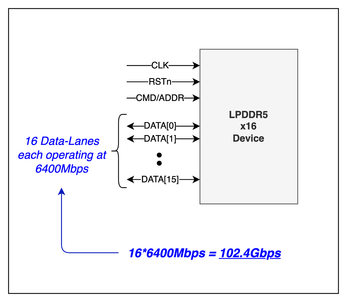
Bandwidth is the theoretical peak performance that a memory can achieve. For example, in LPDDR5 the maximum bandwidth of a memory channel is ~102Gbps.
Each memory channel has 16 data lanes1, with each lane capable of supporting 6400Mbps. So 6400*16 = ~102Gbps. This is the raw bandwidth.
In reality, this bandwidth is not attainable. The actual data rate that can be achieved is called throughput. To understand why the attainable throughput is less than the maximum bandwidth, we need to understand DRAM timing parameters.
What are timing parameters
Due to the physics governing DRAM devices, certain timing constraints or delays have to be observed while performing operations on the memory. The effects of timing parameters on memory bandwidth is best understood in the context of specific memory operations. We’ll next look at the Refresh command and a Read operation.
REFRESH command
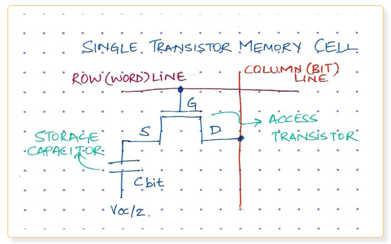
At the lowest level, a DRAM cell is essentially a capacitor that holds charge with a transistor acting as a switch. Since the capacitor discharges over time, it has to be Refreshed periodically to ensure data is not lost.
There are 2 main timing parameters related to the refresh operation.
tREFI (Refresh Interval): This parameter specifies how often the memory has to be refreshed so that data is not lost.
tRFC (Refresh Cycle Time): This parameter specifies for how much time the DRAM is unavailable once it enters Refresh.
For example, in case of LPDDR5,
The memory needs to be refreshed every 3.9us (
tREFI).Once the memory enters refresh it is unavailable for ~200ns (
tRFC).
So, if the memory is unavailable for
~200nsevery3.9us(i.e.,3900ns), then we lose nearly 5% of the bandwidth JUST to Refresh.
200/(3900+200) = 4.8%
Simple READ operation
Going up one level, DRAM cells are arranged in a grid of Rows and Columns. One such grid is called a memory bank.
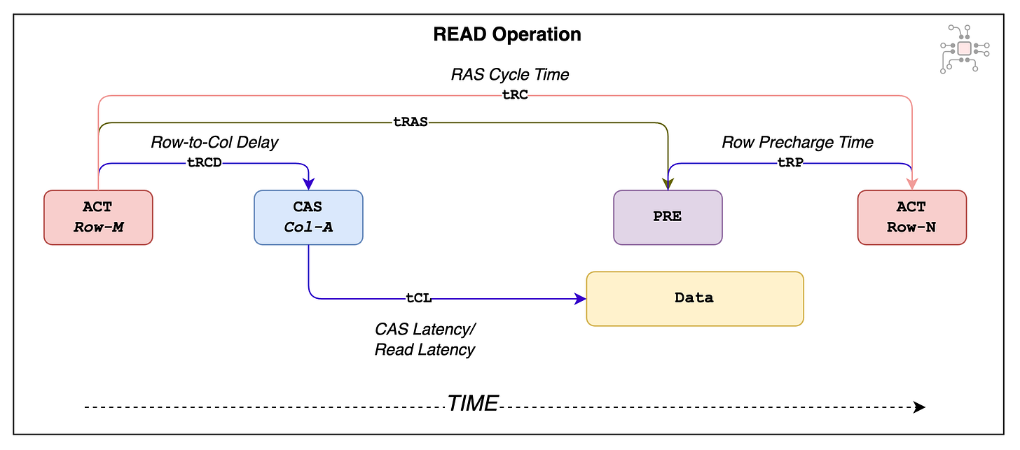
From the outside world, it may look like reading from a memory bank is an atomic operation. But, in reality it is a multi-step process between the processor (memory controller, to be precise) and the DRAM. The 3 steps typically involved in a READ operation are:
Activate (ACT): A portion of the read address identifies which row within the bank the data is stored in. The processor first sends an ACT command to the DRAM to transfer the data from the memory cells into the bank’s Sense Amps.
Column-Address-Strobe (CAS):
The activation process takes some time, so only after a delay of tRCD (Row-to-Column Delay) the column address can be sent to the DRAM.
Then, after a latency of tCL (CAS Latency), the data is returned.
Precharge(PRE):
Before accessing another row within the same bank, the currently open row has to be deactivated. This process is called Precharging.
Once the current row is deactivated, it has to remain idle for tRP time before another row can be activated.
Also, care has to be taken to ensure that the time between two ACT commands is at least tRC. This is the row cycle time.
These timing parameters are illustrated below. As you can see, a basic read operation involves a number of delays and latencies.
In the context of LPDDR5 running at 6400Mbps, tRCD is 18ns and tCL is ~22ns and after all that setup, it takes just 2.5ns to read the data back from that column. So the overhead is substantial.
In the upcoming section we’ll see how hiding these latencies is crucial to extract maximum performance out of the DRAM.
Hiding latencies to maximize throughput
Let’s stick with READ operations and examine 4 different back-to-back read scenarios, and how the performance varies widely for each of them.
Page hits vs page miss
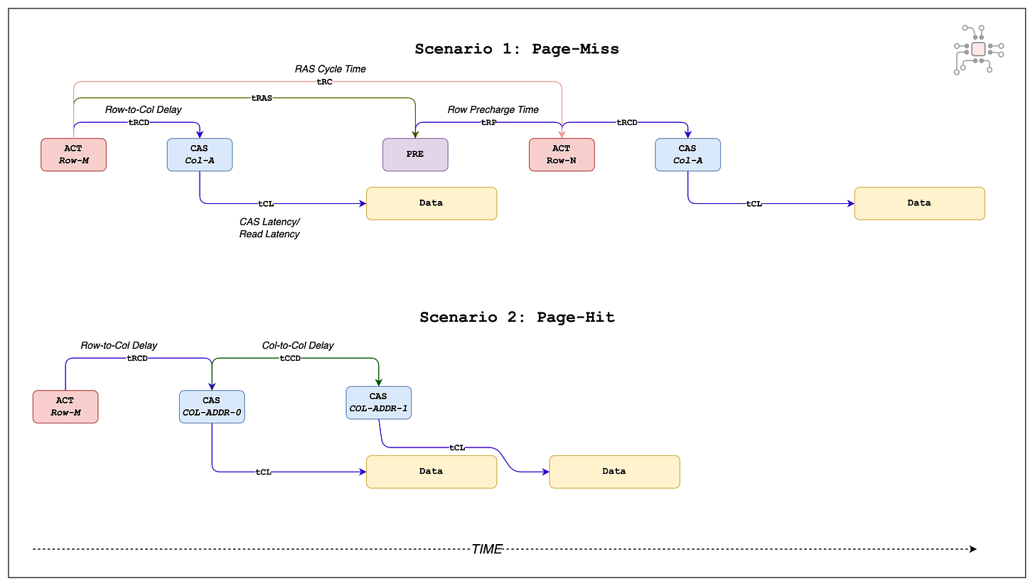
Scenario 1: Back-to-back reads to the same bank but different rows.
Scenario 2: Back-to-back reads to the same bank and same row.
In scenario 1, since the relevant data is located in 2 different rows, after the first row is accessed it has to be deactivated, and the second row has to go through the activation process all over again. This scenario is also called a Page Miss.
But in scenario 2, both the reads have the same row address, only the column address is different. Here the row activation process only happens once. After which, two CAS (column-address-strobes) are sent from the processor and the data is read back. This scenario leads to what is called a Page Hit.
In scenario 2, the two CAS commands are separated by a timing parameter called tCCD (col-to-col delay)
As evident from the figure below, in case of a page miss it takes a lot longer to fetch the data from the DRAM.
Bank Groups vs Banks
While page hits are important, accessing the same bank in back-to-back reads is not good. We can do better to hide some of these latencies, especially the tRCD.
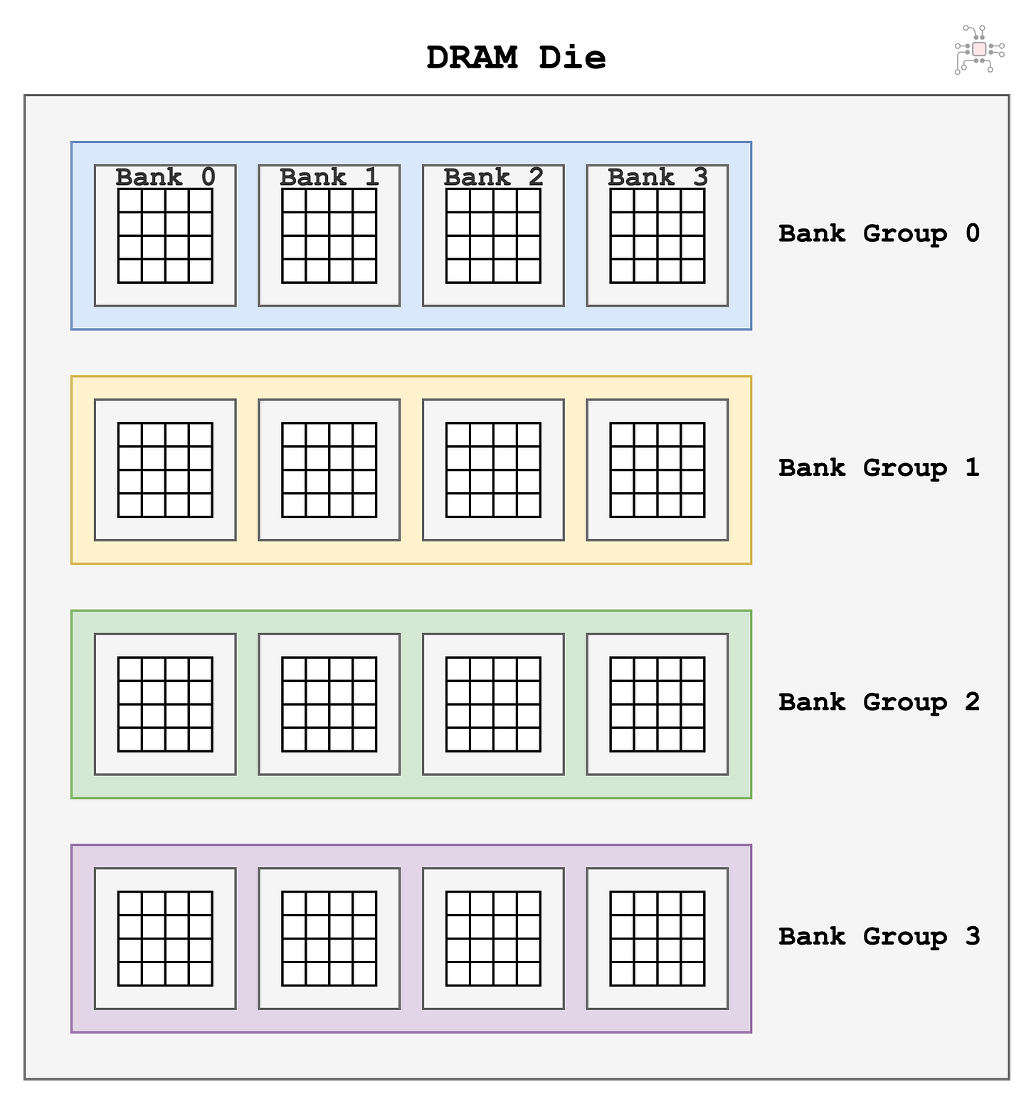
Fortunately for us, the DRAM die is made up of not just one bank but a collection of banks, which are arranged in Bank Groups. Next, we'll look at how bank groups help us improve performance.
Each bank has a set of Sense Amps. They are like different books, you are allowed keep a page (i.e., row) open in each Bank. So, when the memory controller sees two reads to different banks,
It issues an ACTIVATE to the first bank, and while waiting for tRCD (Row-to-Col-Delay) it issues a second ACTIVATE to the second bank and prepares it for the second read. By doing back-to-back reads to different banks, you have allowed the memory controller the opportunity to hide the tRCD latency for the second bank.
Similarly, once the controller issues the CAS (column address strobe) for the first read, it issues the second CAS to the different bank while waiting for tCL (Read Latency).
This process of doing things in parallel reduces the total latency to finish both reads.
This principle of hiding latencies is crucial to extract as much performance as possible out of the DRAM, and fundamentally speaking, the data has to first be stored in a suitable fashion to help the controller hide the latencies.
But, banks and bank groups are not equal. Let’s examine the next two scenarios
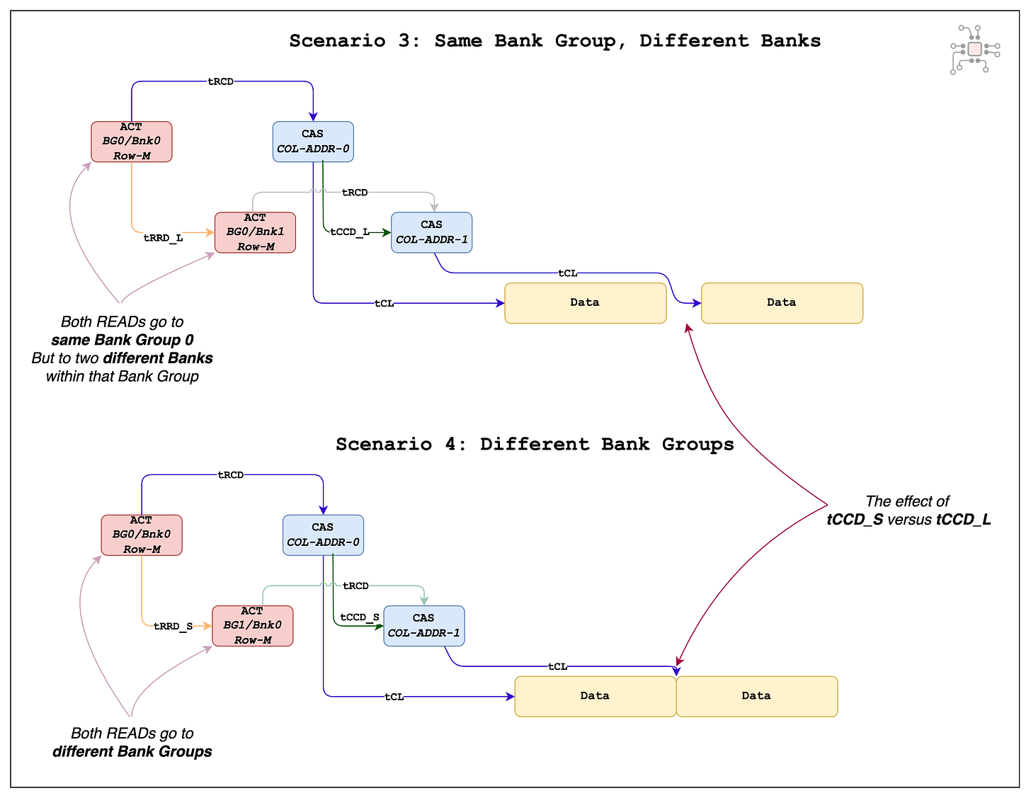
Scenario 3: Back-to-back reads to different banks in the same bank group
Scenario 4: Back-to-back reads to different banks in different bank groups
In scenario 3, since the back-to-back reads go to different banks of the same bank group, the two reads have to be separated by the tCCD_L (Column-to-column-Long) timing parameter. (Which is 4 clock cycles in LPDDR5).
In scenario 4, the back-to-back reads go to different bank groups. In this case, the CAS (column-addres-strobe) commands only need to be separated by tCCD_S (Col-to-col-Short). So scenario 4 ends up being the best case for DRAM performance.
For LPDDR5 operating at 6400Mbps, tCCD_S is 2 clock cycles (2.5ns). That happens to be exactly the amount of time needed to read out the data from a single column. This detail is critical — if you want to keep the data bus fully occupied and extract maximum performance from the memory, two conditions have to be met.
Successive reads should target different bank groups.
A high portion of the accesses should be page hits.
With this setup, you can first issue a sequence of tRRD_S (row activation) commands to open rows across multiple bank groups. Once those pages are active, you can issue a burst of tCCD_S commands to stream data continuously from the open pages.
In this best-case scenario, the memory bus stays busy almost all the time, allowing you to capture roughly 93% of the theoretical bandwidth.
Summary so far …
Timing parameters are a necessary evil. But it is possible to work around some of them by hiding the latencies.
For the best performance, back-to-back reads should be issued to different Bank Groups. This is when the latencies introduced by the timing parameters are the least.
The performance is worst when back-to-back reads are issued to different rows of the same bank.
A basic understanding of timing parameters is necessary to develop an intuition of how good or bad the access pattern is for your workload. Take the time to study the illustrations above, there is a lot of detail in them.
Here’s a convenient cheatsheet of all the timing parameters we discussed above.
🔒 Meta, memory controllers, and estimating performance
In the members-only section,
We’ll take a look at two more timing parameters - tFAW and tWTR, which play a crucial role in performance.
We’ll take a brief look at how memory controllers work, and the structures at your disposal to help maximize throughput.
How companies like Meta and Apple evaluate and study the performance of their DRAM architecture.
Tools and strategies that are used to study performance.
Common mistakes made during performance estimation.
Chiplog is a member supported newsletter. Right now memberships are 25% off, that’s $74/year(~$6/month).


