All DRAM memories, whether it’s HBM3, LPDDR5, GDDR6, or DDR5, are built on the same fundamental concepts. From an engineering perspective, these memories are challenging to work with, and in most ASICs and SoCs (no matter the application — AI training/inference, CPU, GPU, or Networking), performance often ends up beingmemory-bound.
So, in order to design a robust memory subsystem, make these memories run reliably, and squeeze out every bit of performance out of them, you need to understand 3 key dimensions:
PhysicalStructure - Understanding the physical structure is required to efficiently store and retrieve data from the memory. A good data storage architecture is critical to performance.
Timing Parameters - Reading and Writing to DRAM is like a carefully choreographed dance. We are bound by the physics of these devices. Timing parameters dictate the rules that have to be followed while accessing DRAM memories, i.e., how fast you can access the memory, how often they have to be refreshed to retain data, and such.
Initialization and Calibration - Over its lifetime, a DRAM device will be subject to variations in Process, Voltage and Temperatures (PVT). Memory controllers use special circuits and algorithms to periodically tune the interface so it runs reliably in all conditions.
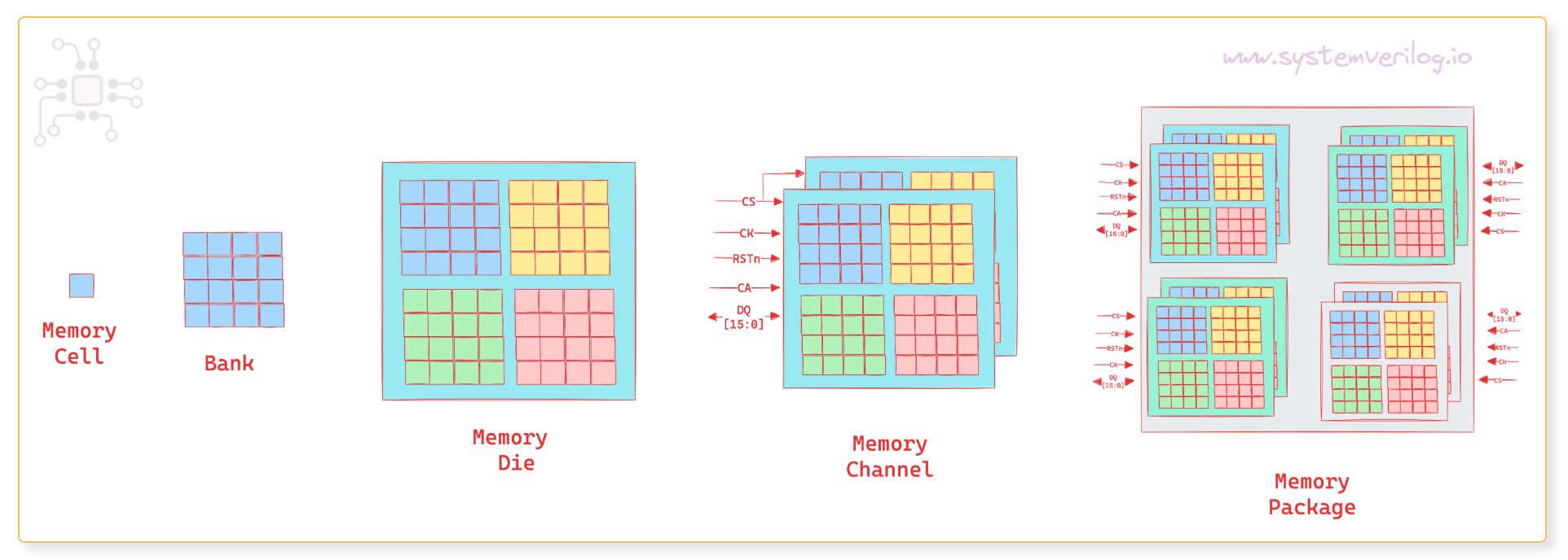
In this post, we will focus on Dimension #1: the physical structure of DRAM. We’ll start from a single DRAM cell and work our way up to a complete package, while discussing ranks, banks, channels, page hits/miss and other terminology.
🔒 For members:
We’ll take a side-by-side look at HBM3E and LPDDR5X — two of the most popular DRAM types that are shipping in volume right now
Explore their structural differences
Understand why HBM’s design delivers such staggering bandwidth compared to LPDDR5
Chiplog is a member supported newsletter. Right now memberships are 25% off. That’s $74/year (~$6/month).
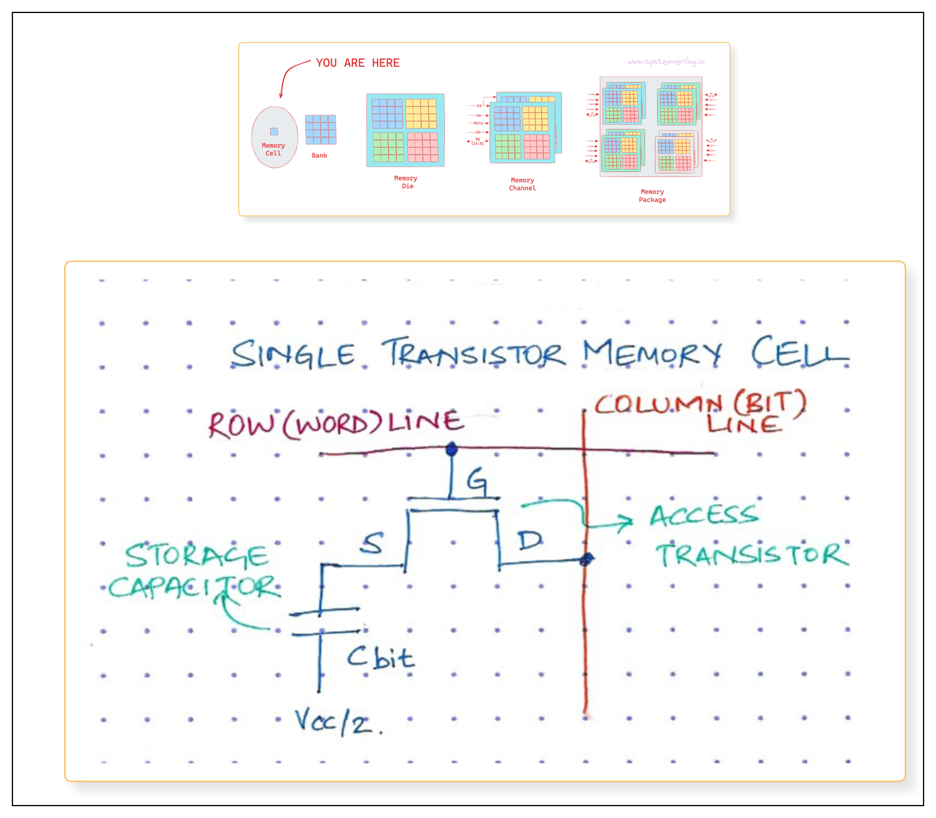
At the lowest level, a memory cell stores 1-bit of information. This cell is essentially a capacitor that holds the charge and a transistor acting as a switch. Since the capacitor discharges over time, the information eventually fades unless the capacitor is periodically REFRESHed. This is where the D in DRAM comes from - it refers to Dynamic as opposed to the Static in SRAM.
Rows, columns, banks
When you zoom out one level, you will see these memory cells arranged in a grid of Rows and Columns. One such grid is called a Bank.
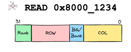
In order to read or write to a specific location in the memory, an address has to be specified. In this address the Bank, Row and Column numbers are encoded.
Address showing different portions — Column, Row, Bank, Rank (More on rank later)
A memory bank is like a book, where
BANK address indicates which book you want to read or write to
ROW address is the page number within that book
COLUMN address is the line number within that page
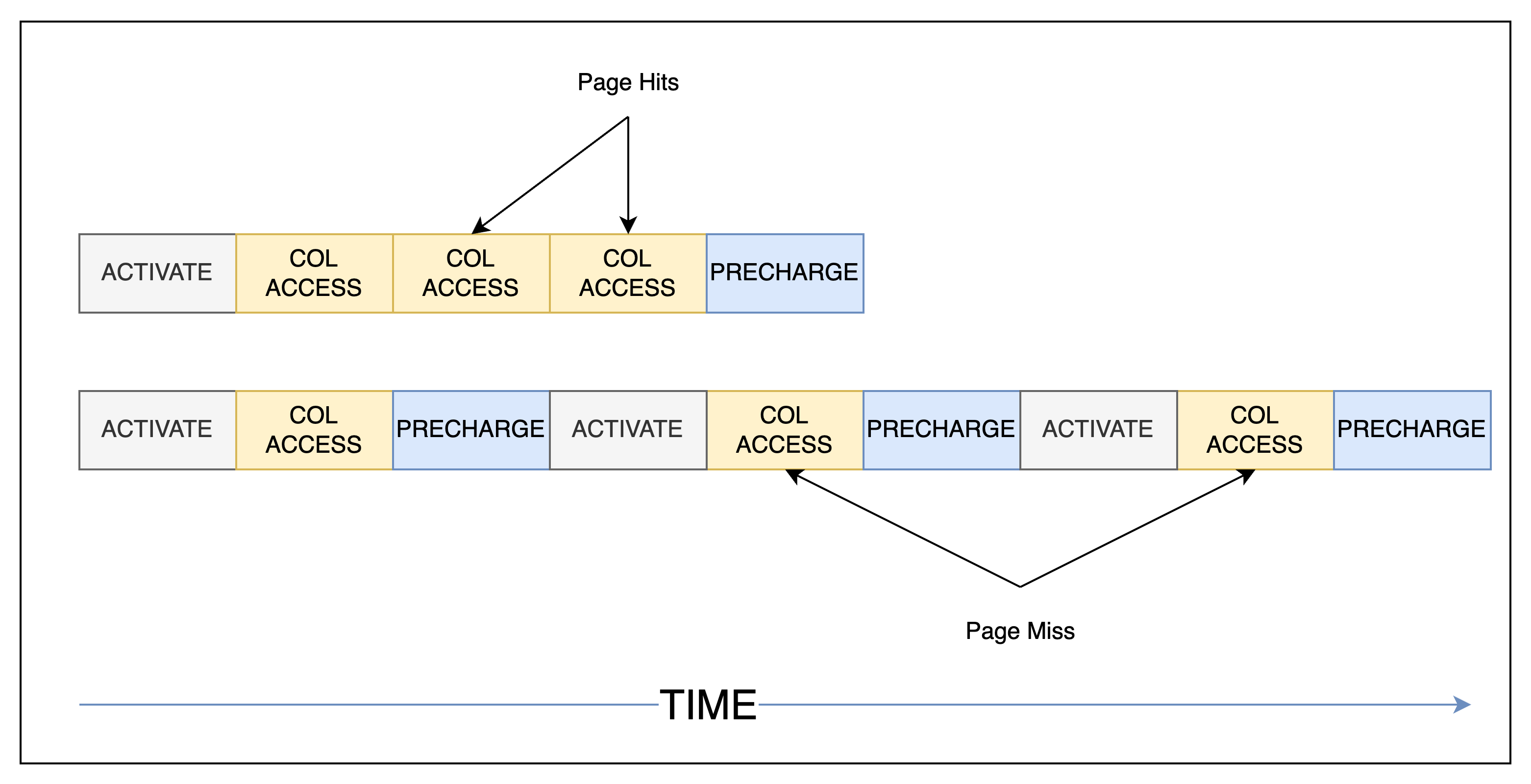
There are 3 distinct phases in accessing a memory:
ACTIVATE: First a Row Address Decoder ACTIVATEs the row number specified in the address, and brings the data into a structure called the Sense Amp. This is equivalent to opening the desired page of the book.
COLUMN STROBE:Then a Column Address Decoder extracts data from a specified column and streams it out. This is the same as locating and reading the line in the open page.
PRECHARGE: Once the access is complete, the Row has to be closed and data in the Sense Amps is returned back into the Row cells. This closing of the row is called PRECHARGE. This is the same as closing the book.
The GIF below shows a Memory READ operation in action.
### SIDE NOTE: Page hits and page miss
You may have heard of "Page Hits" and that it
improves performance. This is indeed correct.
Continuing with our analogy of the DRAM bank
being a book ...
Page hit scenario:
If all the data you are trying to retrieve
are present on the same page, then
+ You can open to the page (ROW address) once
+ Read all the lines (COL addresses)
+ Close the page
Page miss scenario:
If the data you are trying to access are
located in different pages, then you will have to
+ Open the first page
+ Read some lines
+ Close that page
+ Open the next page
+ Read some more lines
+ Close that page
+ ... and so on
Needless to say, there is a significant penaltyto page misses since there are many more ACTIVATEs
and PRECHARGEs to be performed.
Page hits versus page miss
Memory die
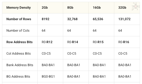
A memory die is one physical wafer and is made up of a collection of banks. Memory vendors such as Micron, Samsung and SK Hynix make memory dies of various densities, depending upon the number of rows, columns and banks.
The table below shows the various densities LPDDR5 memories dies are made in. Notice how larger densities just have more number of Rows.
Standard LPDDR5 memory densities
Memory die
Memory channels
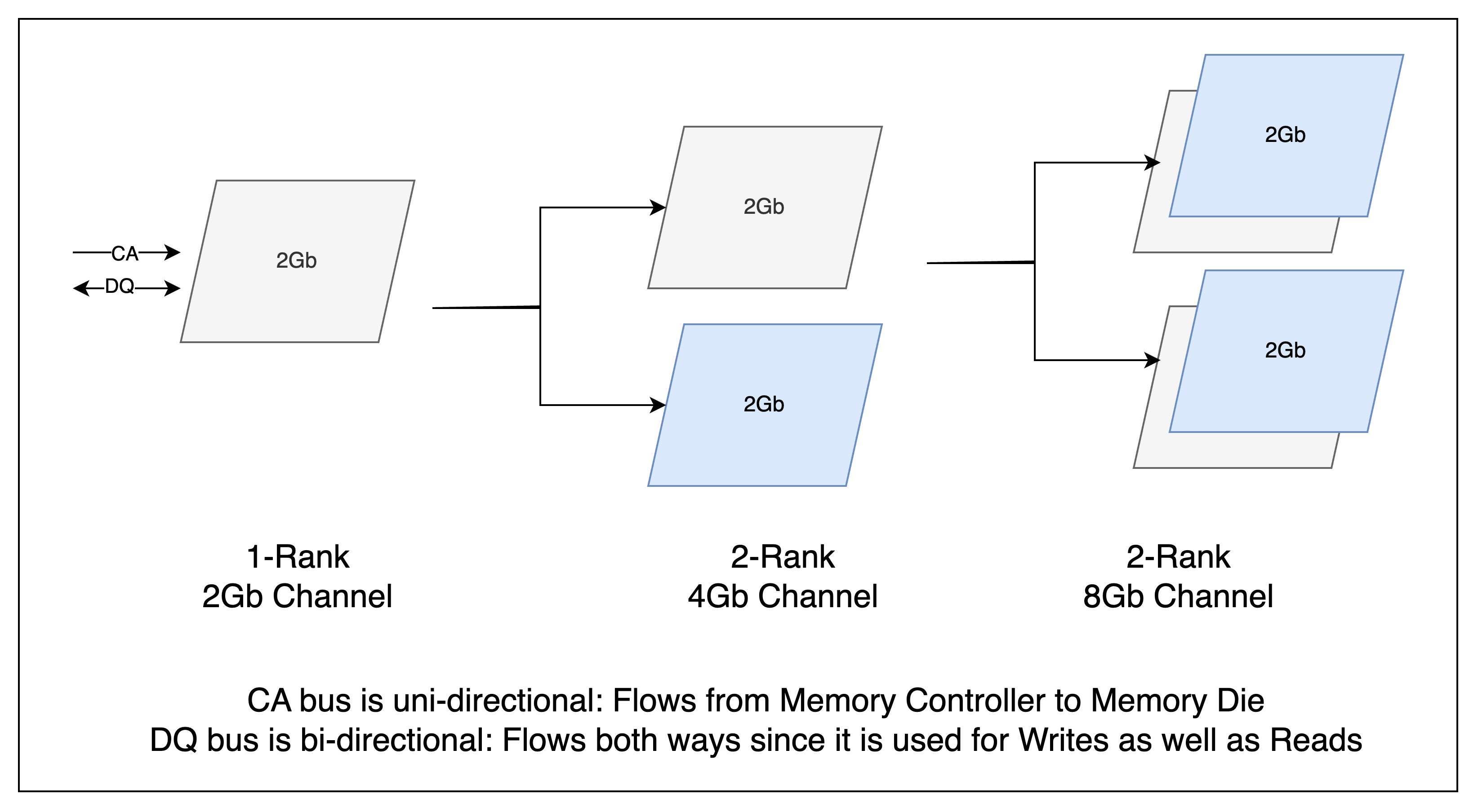
The interface to the Memory is like a pipe … a bundle of wires. This bundle has a name — Command-Address (CA) and Data (DQ) bus.
On one end of this pipe you have the brain (Processor/ASIC with the memory controller — usually called the logic die). At the other end is some arrangement of Memory dies. This pipe with a collection of memory dies at the end of it is called a “channel”, and the image below shows 3 different arrangements of memory dies.
Image shows how a single 2Gb memory die is arranged in different ways to create three different sizes - 2Gb, 4Gb and 8Gb
Memory Package
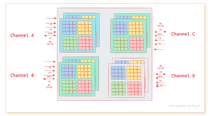
If the memory is a stand-alone unit, like in LPDDR5 or DDR5, then it is packaged so that it can be soldered on the board, or within the main SoC package (Memory-on-Package). This package is made up of multiple-channels. Each channel is connected to a different memory controller and works independently.
A package showing 4 channels with each channel consisting of 2 dies
A Samsung LPDDR5 memory package which can be soldered onto the PCB
Performance
I’ll wrap up the free portion of this article with a quick discussion on performance.
When deciding the memory architecture for an SoC and deciding which memory type to use (HBM, LPDDR, DDR or GDDR), you really only have 3 main levers to pull with regard to performance. (Of course, cost, power, and availability are important factors that guide this decision too.)
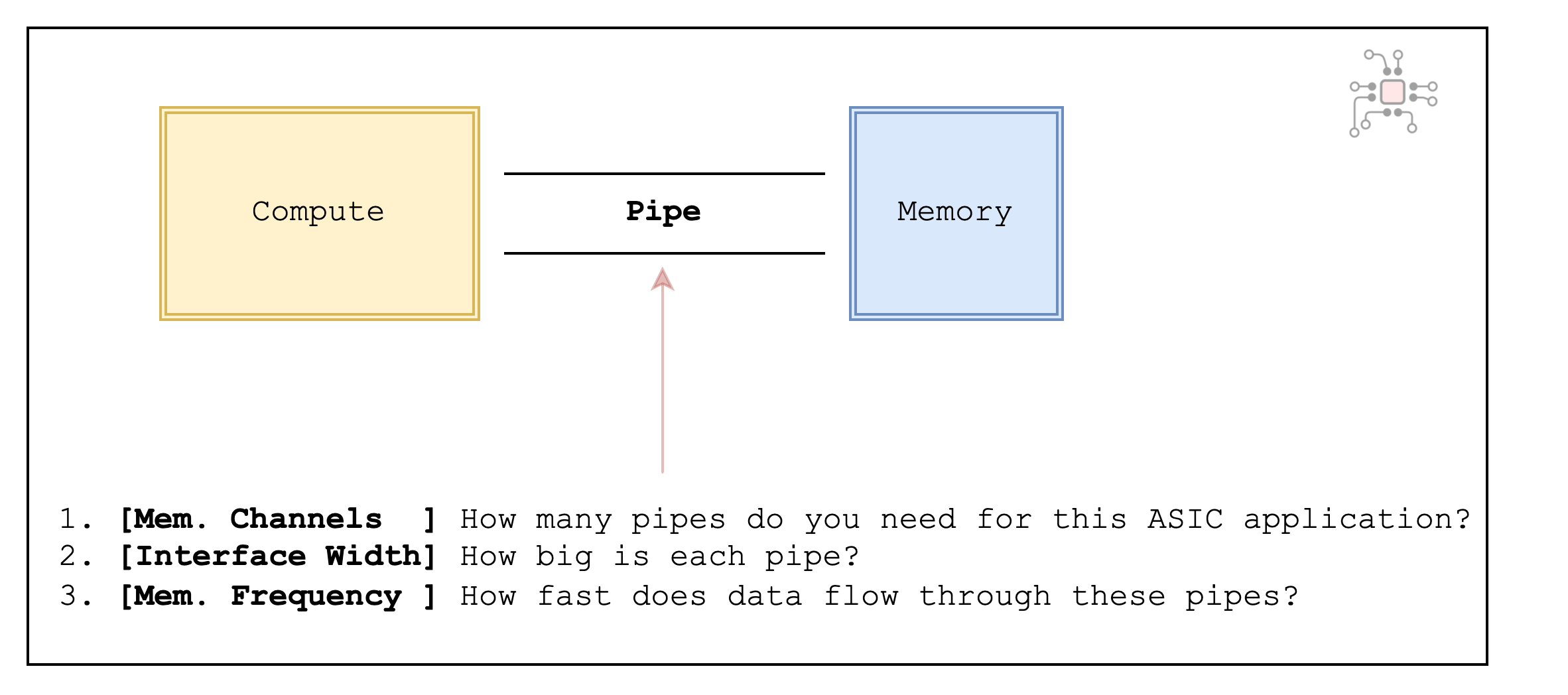
Using the analogy of the compute die being connected to the memory through a pipe, we can ask 3 questions:
3 questions to ask when deciding which memory type to use
1. How many pipes? (Number of memory channels)
If each memory channel delivers 10GB/s of bandwidth per channel, then you have to first decide how many channels are required for your SoC’s application. For instance, if you require 40GB/s of total bandwidth, then you will need four channels.
Each channel needs its own memory controller on the logic/compute die, which eats up both die area and beachfront. Beachfront is the Chip edge real estate where I/O interfaces live. A very precious resource, and something we’ll dive into in the next article (another reason to subscribe if you haven’t already!).
2. Size of each pipe? (Memory interface width)
The memory interface width dictates the number of data (DQ) bits that can be transmitted in parallel. The wider the DQ bus, the greater the bandwidth offered by the memory since more bits can be transported between the compute die and the memory in one clock cycle.
3. How fast does data flow through these pipes? (Memory frequency)
DRAMs can be operated at various frequencies, for example LPDDR5 can run at a maximum 6400Mbps, but also at 3200Mbps and 5400Mbps. But cranking the dial to the max isn’t always the feasible.
Higher frequencies draw more power, are harder to run reliably, and can introduce signal integrity headaches. That means your system design and cooling requirements also get more complex.
To balance performance with thermals and stability, techniques like Dynamic Frequency Scaling (DFS) are used to keep the TDP in check. But this complicates software design.
Page Hits & Data Architecture
Any discussion on performance is incomplete without talking about Data Storage Architecture.
Well-structured storage and retrieval patterns can significantly improve how well the memory bandwidth is utilized. Even with the best hardware, the wrong access patterns can leave much of the memory bandwidth untapped.
🔒 Comparing HBM3E versus LPDDR5X
The rest of this post is for members.
We’ll take a side-by-side look at HBM3E and LPDDR5X — two of the most popular DRAM types that are shipping in volume right now
Explore their structural differences
Understand why HBM’s design delivers such staggering bandwidth compared to LPDDR5
Right now memberships are 25% off. That’s $74/year (~$6/month). With this membership, you’ll be supporting chiplog.io.