

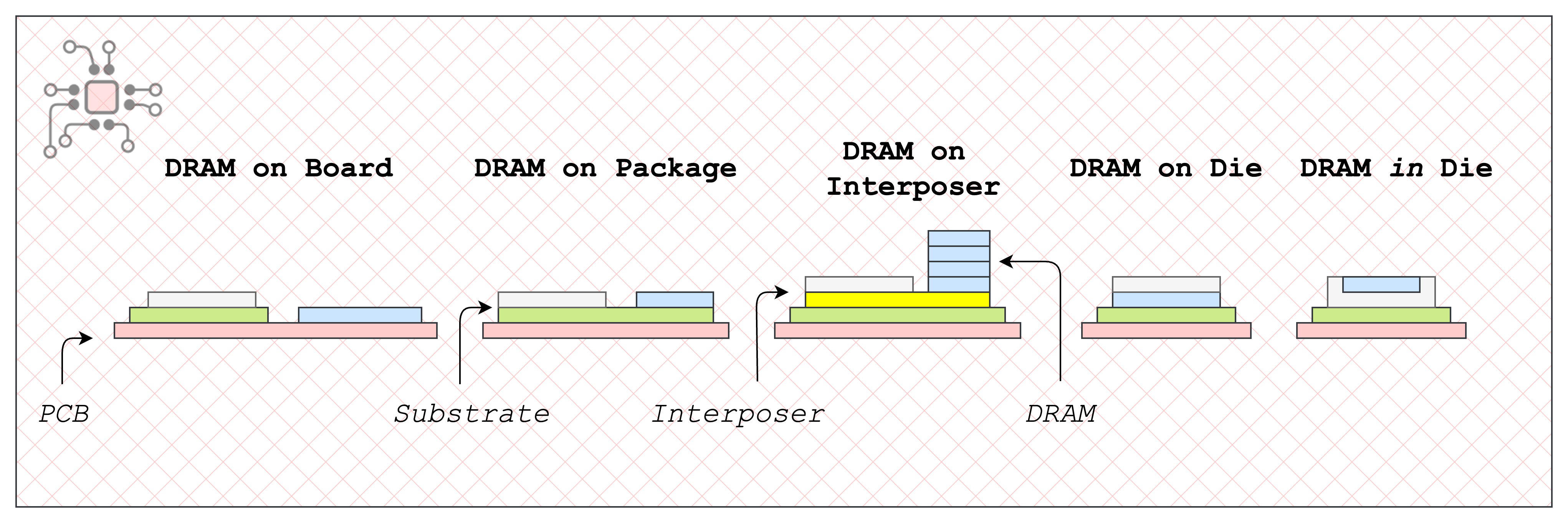
5 different ways DRAM and Compute are integrated
Examples of how GDDR, DDR, LPDDR, HBM and 3D DRAM are integrated with compute

In the last two posts, we dug into the fundamental building blocks of DRAM and got into the weeds with DRAM timing parameters and how it affects performance. Today’s post is lighter and more visual. We’ll break down how modern systems are built with different types of DRAM: DDR, GDDR, LPDDR, HBM, 3D DRAM and eDRAM.

I’ve categorized the sections based on where the memory physically sits relative to the compute/processor die:
DRAM on the Board – Memory soldered on the PCB. Common with DDR, GDDR, and sometimes LPDDR.
DRAM on Package – Memory-on-Package (MoP) and Package-on-Package (PoP) configurations, used with LPDDR.
DRAM on Interposer – Found with HBM.
DRAM on Die – Early look at 3D-DRAM. (d-Matrix, the company I work for, had a big announcement on this just last week.)
DRAM in Die – Embedded DRAM.
🔒 For Members
A brief comment on hybrid bonding.
Deep dive into NVIDIA Grace CPU’s LPDDR5X memory complex
The Grace CPU is arguably more interesting than Hopper or Blackwell GPUs.
Grace uses special off-catalog DRAM components, and I’ll walk through why that is and what makes them unique.
NVIDIA is exercising its special relationship with Micron, and the topology is changing from the Grace-Hopper (GH) super chip to the latest Grace-Blackwell (GB) motherboards.
A comparison of NVIDIA Hopper versus Blackwell HBM complex.
Chiplog is a reader supported newsletter. Right now memberships are 25% off. That’s $74/year (~$6/month).
Acknowledgement
This article wouldn’t have been possible without the excellent images from TechPowerUp and ServeTheHome. Many thanks to them for their fantastic work.
DRAM on Board (DDR & GDDR)
This type of memory integration is the most common. We see it in laptops, desktops, and servers. In this setup, the DRAM package is either soldered directly onto the PCB or first mounted onto a smaller daughter card (a DIMM module) that plugs into the main PCB through a socket. The processor and memory communicate through traces routed across the motherboard. Here are a few examples.
Example 1: GDDR in NVIDIA GeForce cards
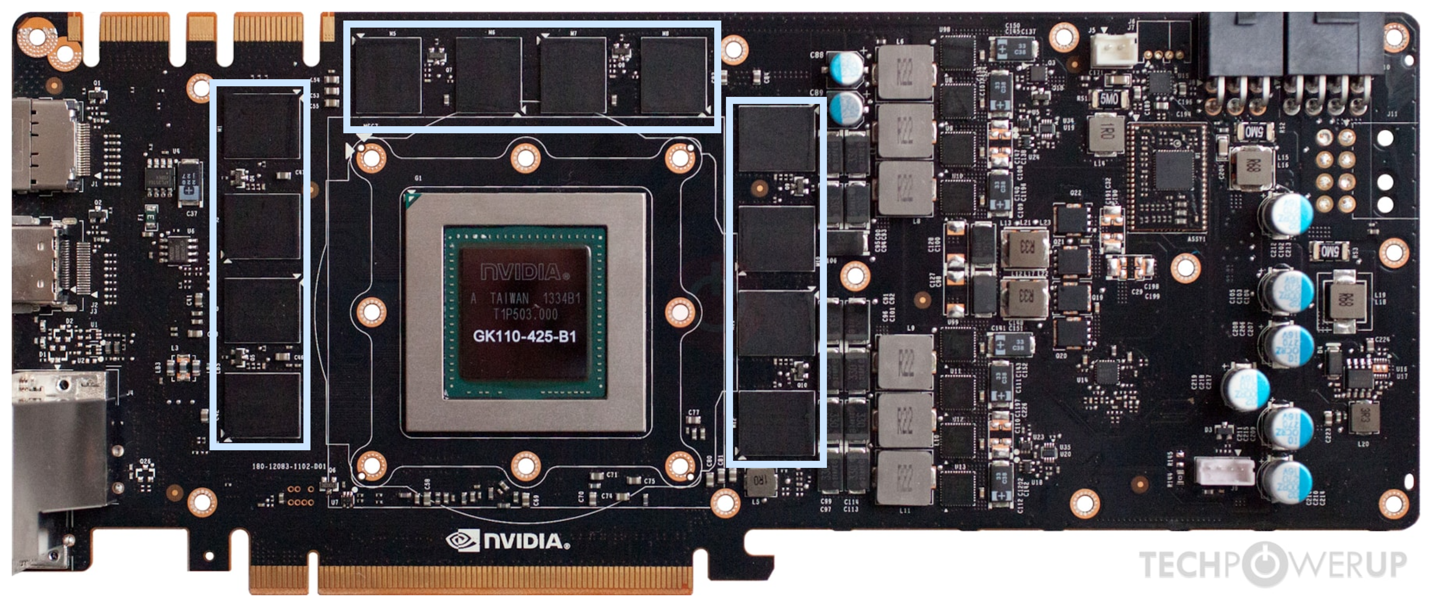
Below are annotated images from three generations of NVIDIA graphics cards. In each case, GDDR memory is soldered directly onto the board. The DRAM devices are width-cascaded, forming a wide memory interface that the GPU can access in parallel.
NVIDIA GTX 780 Ti with GDDR5
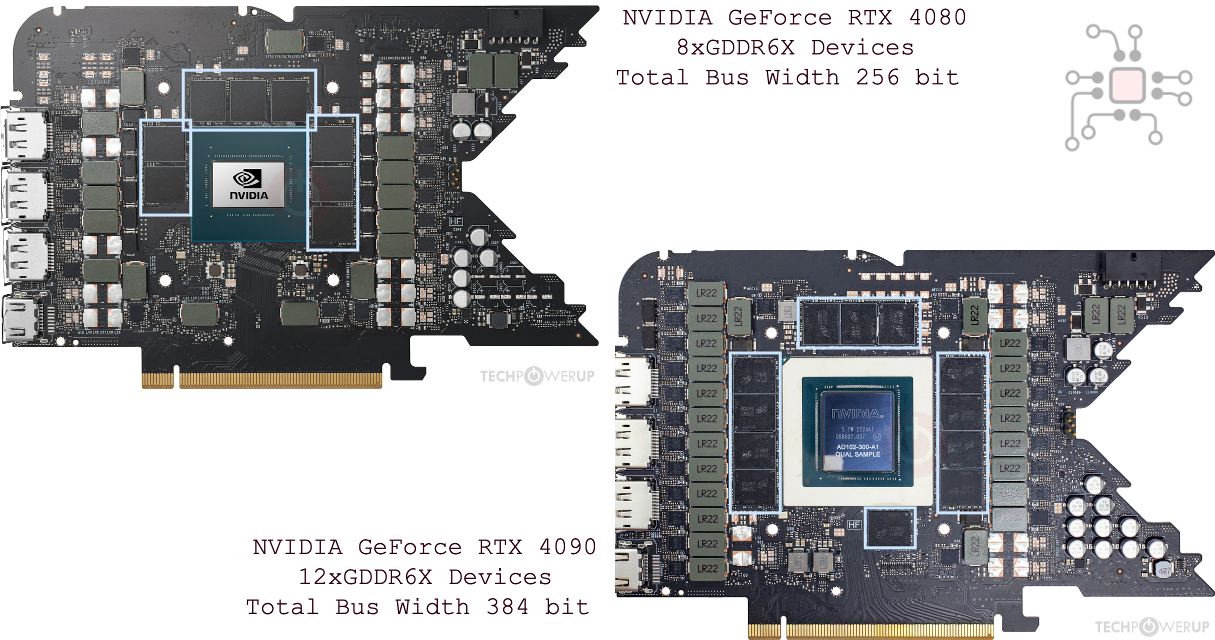
NVIDIA RTX 4080/4090 with GDDR6X
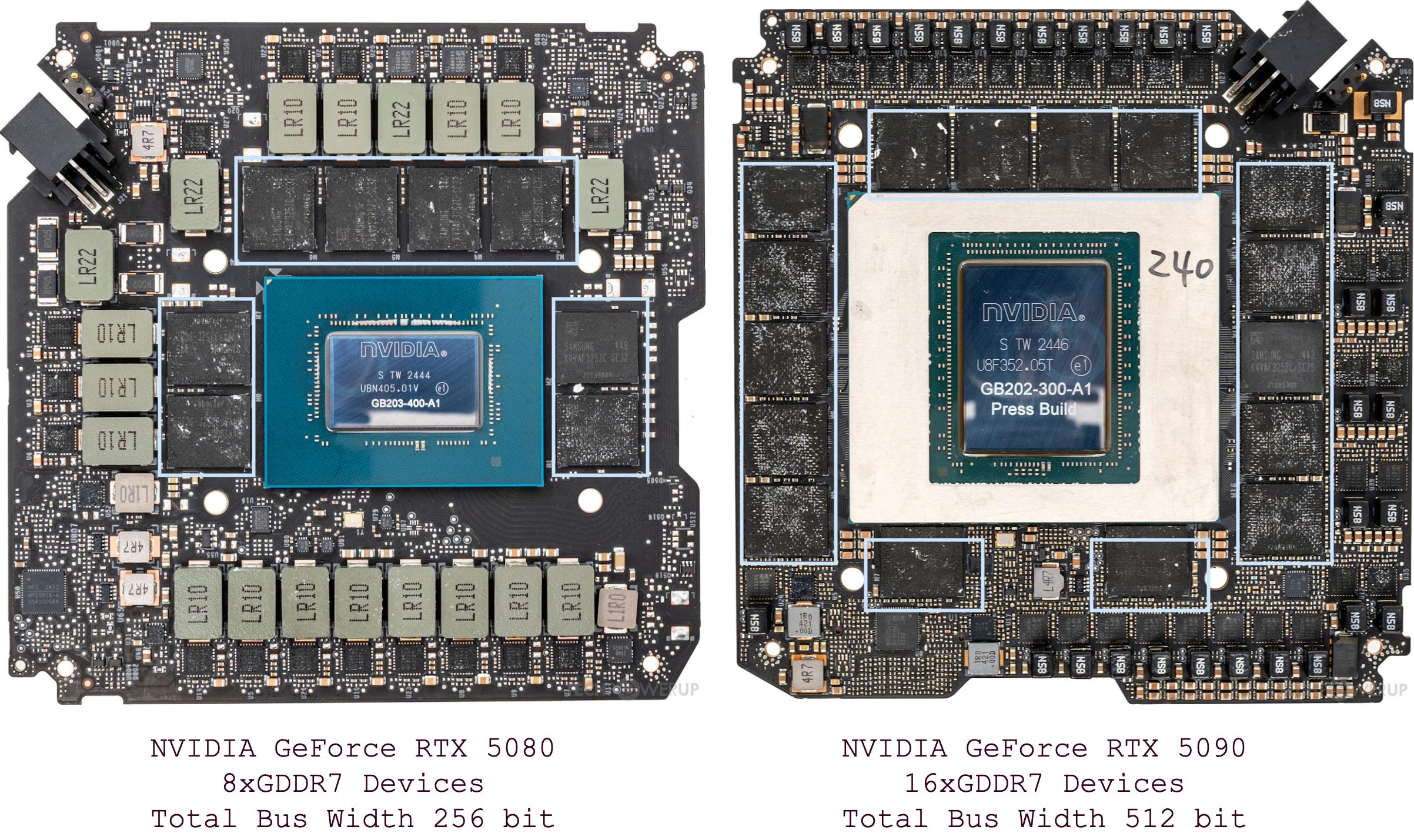
NVIDIA RTX 5080/5090 with GDDR7
The GTX 780 Ti is fed by 12 GDDR5 chips, each with a 32-bit data bus. Together, these 12 devices provide the GPU with a 384-bit wide memory interface.
Next, let’s compare the RTX 4080 and RTX 4090.
The RTX 4080 uses 8 GDDR6X devices, each with a 32-bit data bus, giving the GPU a 256-bit wide memory interface. With each device providing 2 GB of capacity, the card has a total of 16 GB of memory.
In comparison, the RTX 4090 has 12 GDDR6X devices for a 384-bit interface, with a total capacity of 24 GB.
Finally, the latest generation RTX 5080 and 5090 move to GDDR7. The 5080 is equipped with 8 devices for a 256-bit bus, while the 5090 doubles that with 16 devices, delivering a massive 512-bit bus width.
While it may seem obvious, it’s worth emphasizing that every additional DRAM device comes at a cost. It consumes PCB area, requires dedicated memory controller logic on the processor die, and increases routing complexity on the board.
Eventually, physical limits take over, you either run out of PCB real estate or processor die area to accommodate more controllers. These constraints ultimately define the maximum bus width and the upper bound on memory capacity for a given graphics card.
Example 2: DDR5 in Intel 6700/6500 SuperMicro cards
From the graphics cards examples, we saw that even at the very high end, memory tops out at around 32 GB of DRAM capacity. But 32 GB isn’t much if your application demands more. So how do you scale beyond that?
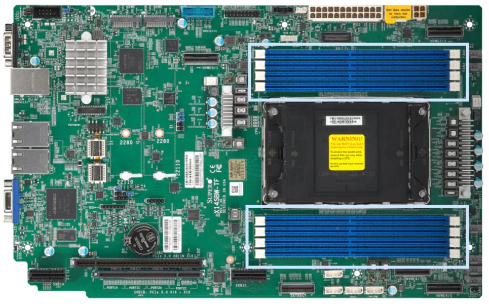
This is where memory modules come in, a form of integration more common in CPUs. For example, this Micron 128 GB DDR5 RDIMM, priced at roughly $1,000, packs 40 DDR5 DRAM devices (20 soldered on the front and 20 on the back). This dual-sided design is what gives it the name Dual Inline Memory Module or DIMM.

These modules then plug into the system’s motherboard. For instance, a Supermicro X14 server board designed for Intel’s latest 6700-series CPUs supports 8 DIMM slots. Fully populated with 128 GB sticks, the system reaches a total capacity of 1 TB (1024 GB) of ECC protected DRAM.
The scaling method here is different from GPUs. While GPUs expand capacity by width-cascading DRAM devices (wider buses), DIMMs expand via depth-cascading, adding more memory devices behind the same interface width. This approach increases total memory capacity without widening the bus.
The Intel 6700 CPU, for instance, supports 8 DDR5 memory channels, and system capacity can be scaled by populating those channels with different DIMM sizes.
GPUs optimize for bandwidth, CPUs optimize for capacity. The type of integration reflects the workload priorities. Fast, parallel access for GPUs versus large, expandable memory pools for CPUs.
Types of DIMMs
There are several different types of DIMMs to choose from, depending on form factor and functionality.
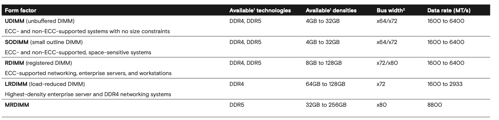
Form factor: A standard DIMM measures 133.35 mm × 31.25 mm, whereas a SODIMM (Small Outline DIMM) is more compact at 69.6 mm × 30 mm, making it suitable for laptops and other space-constrained devices.
Functionality: Different applications impose different requirements. Laptops are cost-sensitive, so unbuffered DIMMs (UDIMMs) are usually sufficient. Servers in data centers, however, demand higher reliability and capacity, so they use ECC-protected RDIMMs (Registered DIMMs). In RDIMMs, a chip called the RCD (Register Clock Driver), located on the DIMM module, buffers and regenerates critical signals, like clocks, before reaching the DRAM components. This improves signal integrity and allows for larger, more stable memory configurations.
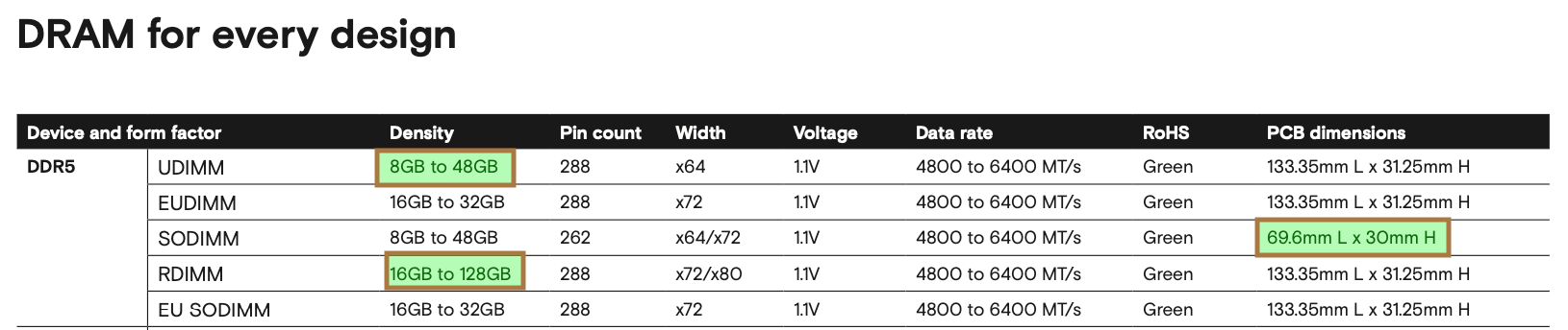
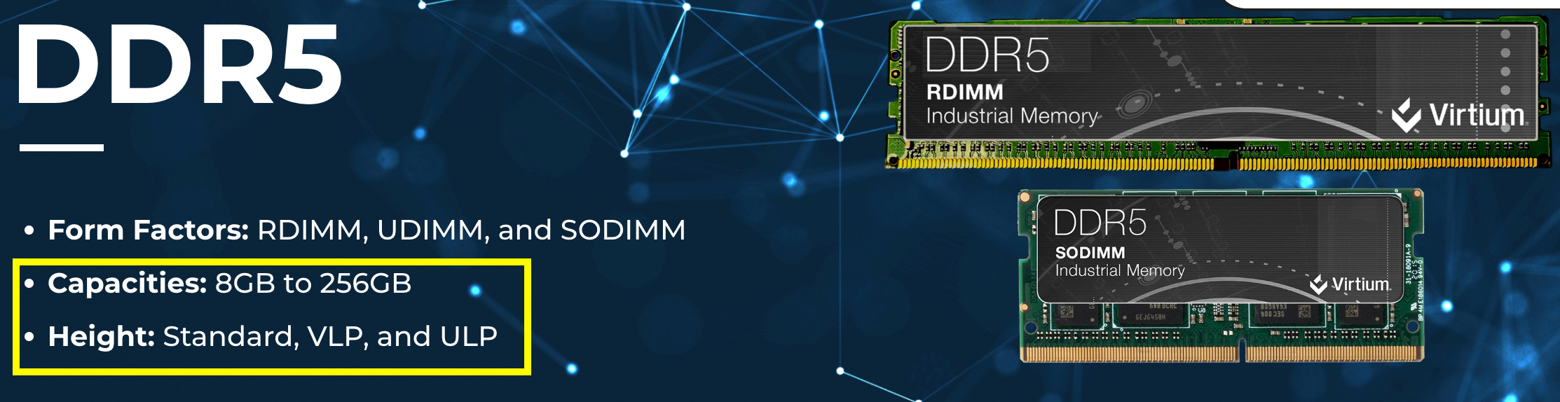
Beyond standard offerings, specialized vendors such as Virtium and Smart Modular provide custom DIMM modules. They can even source DRAM components from vendors like Micron or Samsung and build modules tailored to specific needs.
For example, Virtium manufactures VLP (Very Low Profile) and ULP (Ultra Low Profile) DIMMs to reduce z-height in space-constrained systems. These are not available in Micron’s catalog.
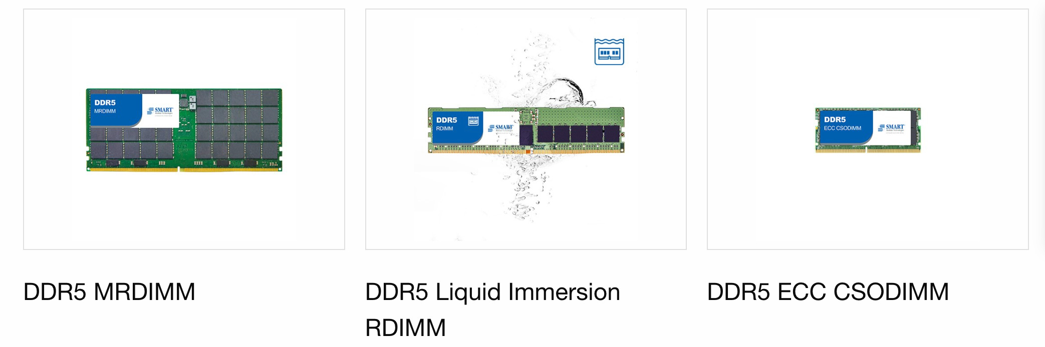
Smart Modular, on the other hand, offers Liquid Immersion DDR5 modules and ECC “C” SODIMMs, which regenerate and amplify the host clock signal for even stronger signal integrity.
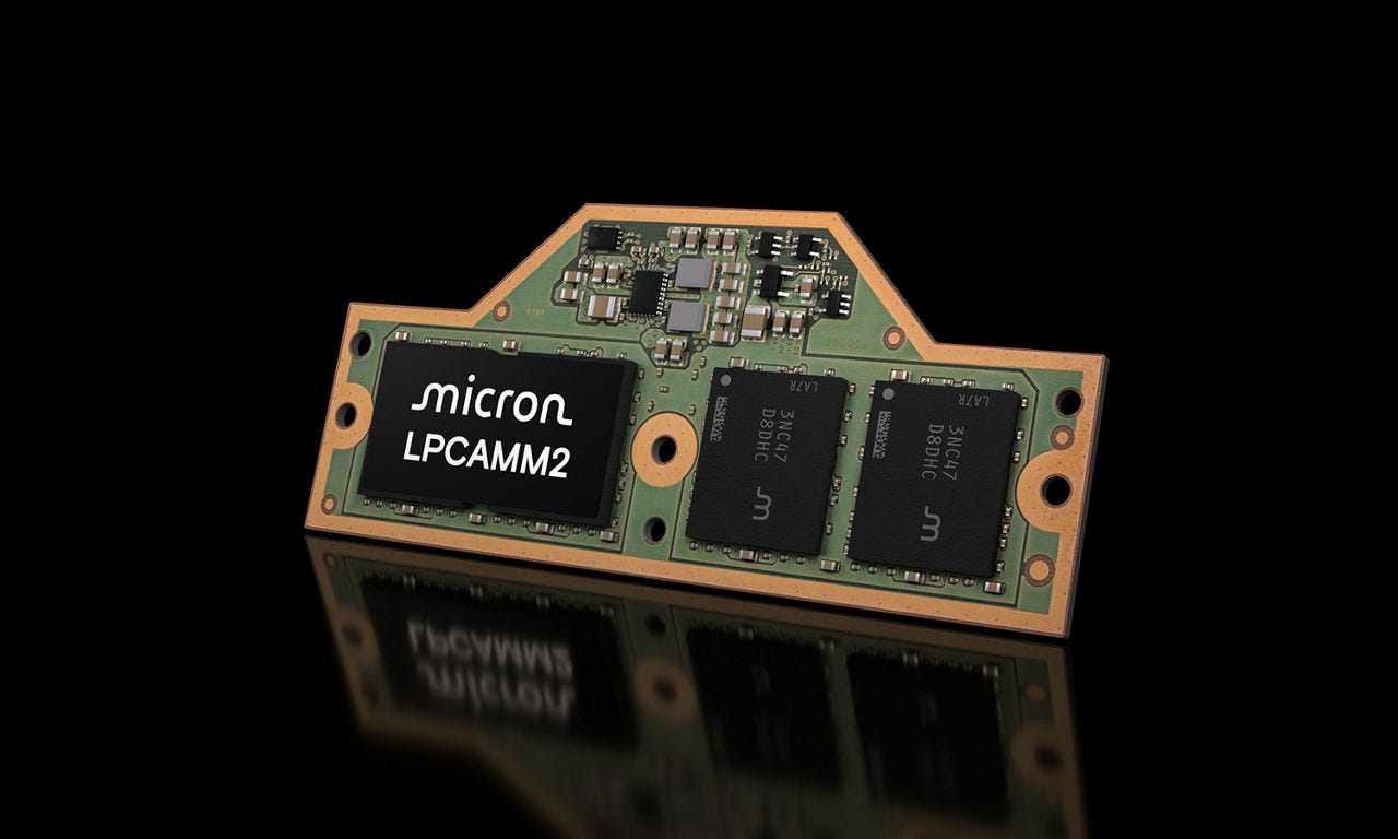
DRAM on Package (LPDDR)
Like GDDR and DDR5, LPDDR memory can be directly soldered onto the PCB or mounted on a LPCAMM module (Low Power Compression Attached Memory Module) and then attached to the motherboard.
However, the more common and increasingly important approach is the style used in Apple’s M-series and A-series SoCs, bringing LPDDR DRAM closer to the processor through advanced packaging.
Memory-on-Package MoP (or On-Package Memory OPM)
In Intel’s Meteor/Lunar Lake and Apple’s M-series chips, LPDDR DRAM and the logic die share the same package substrate. The dies are connected through wires routed within the substrate itself.
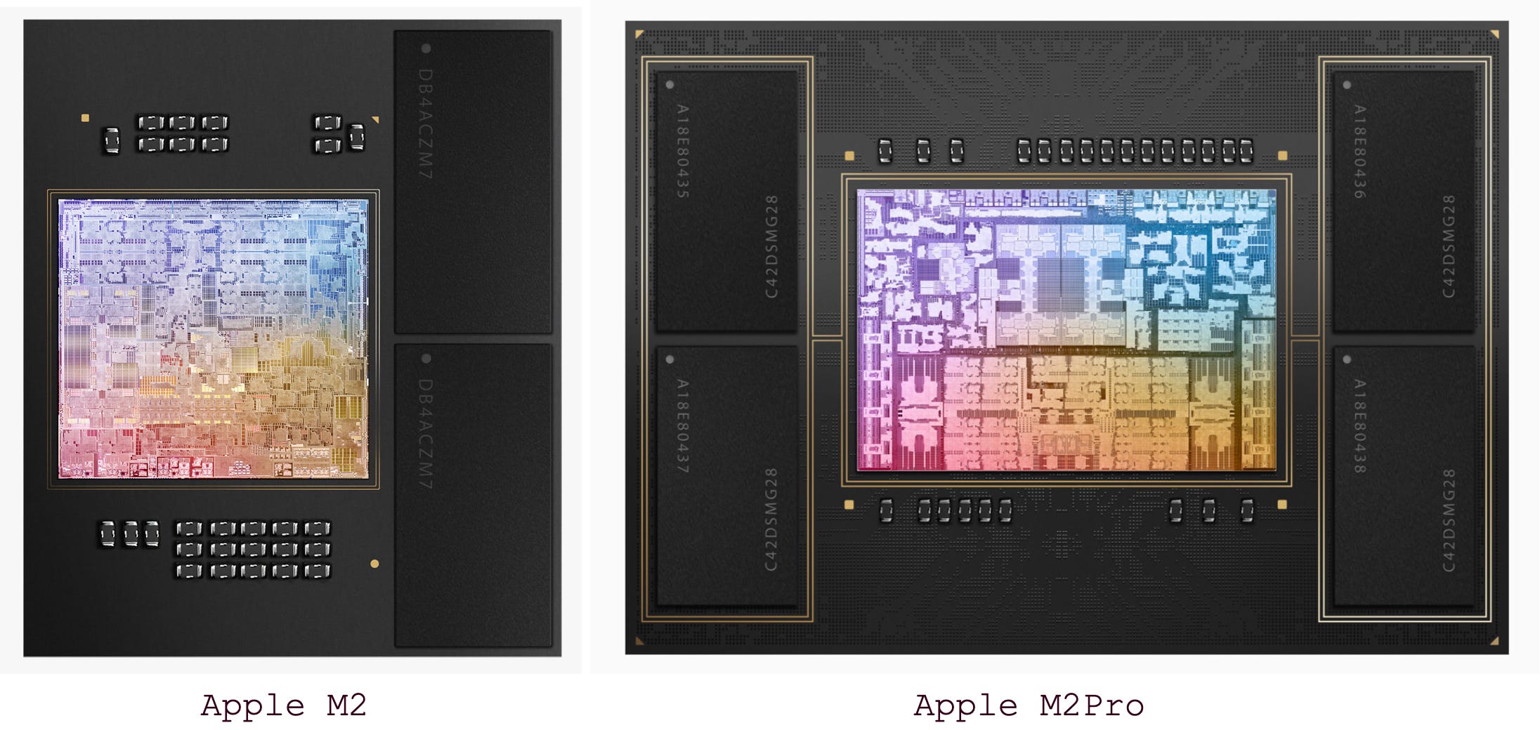

Tightly integrating the memory and logic die sacrifices the flexibility of PCB-based DRAM (where modules can be swapped or scaled), but it saves valuable PCB area. That space can then be repurposed, for example, to fit a larger battery or to reduce the number of PCB layers, lowering assembly and cost.
Package-on-Package (PoP)
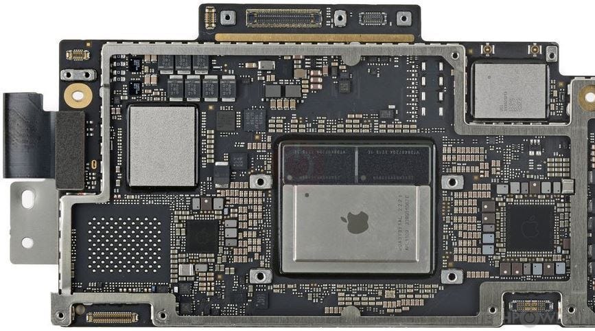
Chips that go into phones, such as Apple’s A-series processors, Qualcomm Snapdragon, and Samsung Exynos, take integration a step further. Here, the DRAM package is physically stacked on top of the SoC. This PoP design tightens the coupling between compute and memory, minimizing the footprint even further.
Below is a snippet from TechInsights’ A14 Bionic package breakdown, which illustrates this approach in practice:
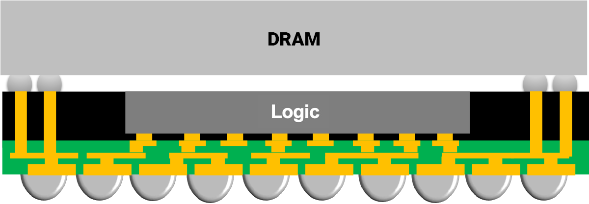
[A14 Bionic uses] package-on-package (PoP) assembly using TSMC’s integrated fan out (InFO) technology.
The top package contains four DRAM dies configured in two stacks of two dies. The memory is wire bonded to a printed wiring board (PWB) ball grid array (BGA). The BGA is connected to the bottom of the package by through molding vias (TMVs).
DRAM on Interposer (HBM)
With HBM, the integration gets even tighter than LPDDR’s Memory-on-Package. Instead of sitting on the substrate (as in MoP), the compute die and DRAM stacks are placed side by side on an interposer. A setup commonly called 2.5D integration.
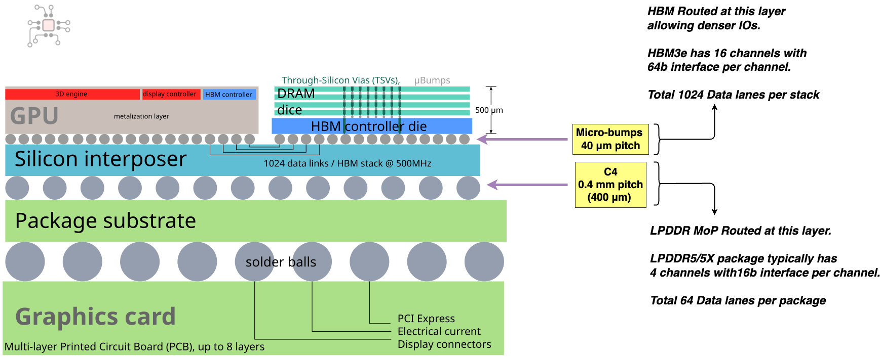
The biggest advantage of using an interposer is routing density. Interposers support much finer connections than substrates. The compute die and HBM stack connect through micro-bumps, while substrates rely on larger bumps called C4 (Controlled-Collapse Chip Connections). To put numbers on it, micro-bump pitch is around 40 μm, compared to 400 μm (0.4mm) for C4 bumps, an order of magnitude tighter. That tighter pitch means you can route far more wires across the interface.
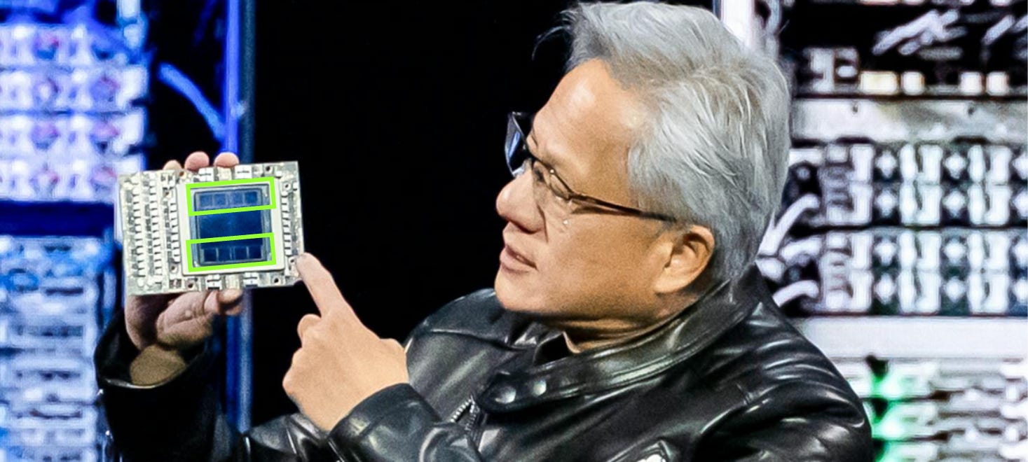
This density shows up in bandwidth. HBM3e provides 1024 data lanes per stack, and HBM4 will double that to 2048. For example, NVIDIA’s Blackwell GPU integrates eight stacks of HBM3e, giving a combined bus width of 8,192 lanes. Each stack can deliver roughly 1 TB/s of bandwidth, which adds up to a staggering ~8 TB/s total.
DRAM on Die (3D DRAM)
The next step beyond HBM’s 2.5D architecture is 3D DRAM. At d-Matrix (where I work), we had an exciting announcement about this.
In this approach, the DRAM is attached directly to the logic die like the interposer. The image below (from our public release) illustrates this integration.

As some of the coverage around our announcement noted, 3D DRAM holds tremendous promise for pushing bandwidth and efficiency even further.
Silicon Angle
According to Bhoja [CTO], by combining 3D DRAM with its specialized interconnects, Raptor will be able to smash through the memory wall and unlock significant gains in terms of AI performance and cost-efficiency. He said the company is targeting an ambitious 10-times improvement in memory bandwidth and 10-times better energy efficiency with Raptor when running inference workloads, compared with existing HBM4 memory technology.
“These are not incremental gains — they are step-function improvements that redefine what’s possible for inference at scale,” Bhoja said.
Block And Files
“Our next-generation architecture, Raptor, will incorporate 3DIMC into its design – benefiting from what we and our customers learn from testing on Pavehawk. By stacking memory vertically and integrating tightly with compute chiplets, Raptor promises to break through the memory wall and unlock entirely new levels of performance and TCO.”
I’ll leave it at that for now. For the latest updates, keep an eye on d-Matrix or follow me on LinkedIn and X.
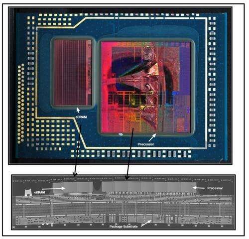
DRAM in Die (eDRAM)
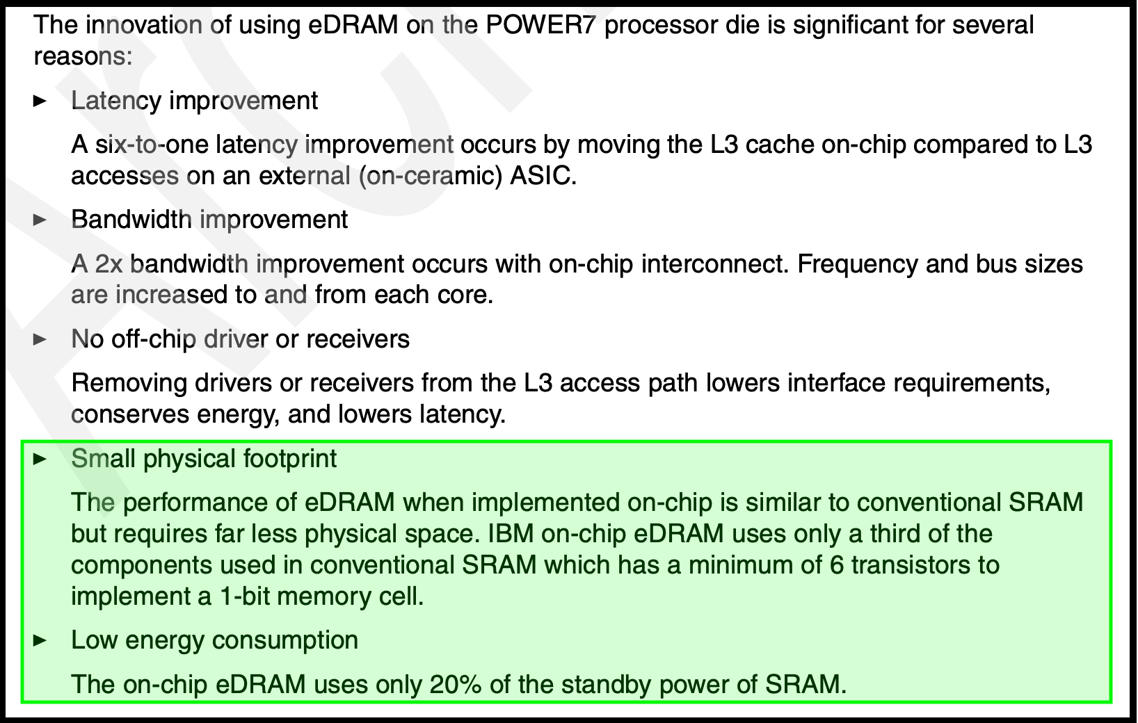
The last chip I worked on with embedded DRAM (eDRAM) was back in the late 2000s and early 2010s, when IBM was building chips on 32nm and larger nodes.
In IBM’s eDRAM, the DRAM cells are part of the logic die itself (similar to how SRAM is integrated) and are built using deep trench capacitors. That means the DRAM cells are fabricated in the same process node as the rest of the chip.

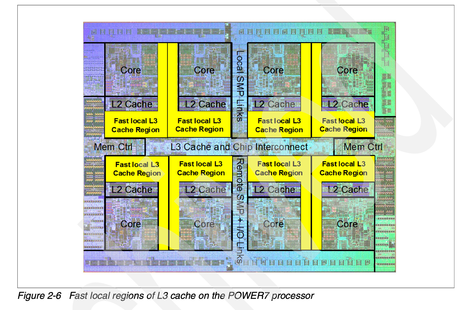
IBM’s Power7 and Power8 processors used eDRAM for their L3 cache
You might also remember it from Microsoft’s Xbox 360, which used eDRAM for graphics. Intel’s Haswell generation also advertised eDRAM, though in that case it was implemented differently, the eDRAM was a separate chip integrated with the CPU through a Multi-Chip Module (MCM) approach.
In a nutshell
This diagram summarizes the types of DRAM integrations we’ve discussed this far.
🔒 Hybrid bonding, Grace, Hopper, Blackwell
In the members-only section, we’ll dive into:
A brief comment on hybrid bonding.
A deep dive into NVIDIA Grace CPU’s LPDDR5X memory complex. How NVIDIA is exercising its special relationship with Micron, and how the motherboards are evolving from the Grace-Hopper (GH) to Grace-Blackwell (GB) systems.
A comparison of NVIDIA Hopper vs. Blackwell HBM complexes.
Chiplog is a member supported newsletter. Right now memberships are 25% off. That’s $74/year(~$6/month).