


In the past few months there is a clear trend emerging with AI inference accelerators. Several companies have teased stacking DRAM and compute as part of their roadmap.
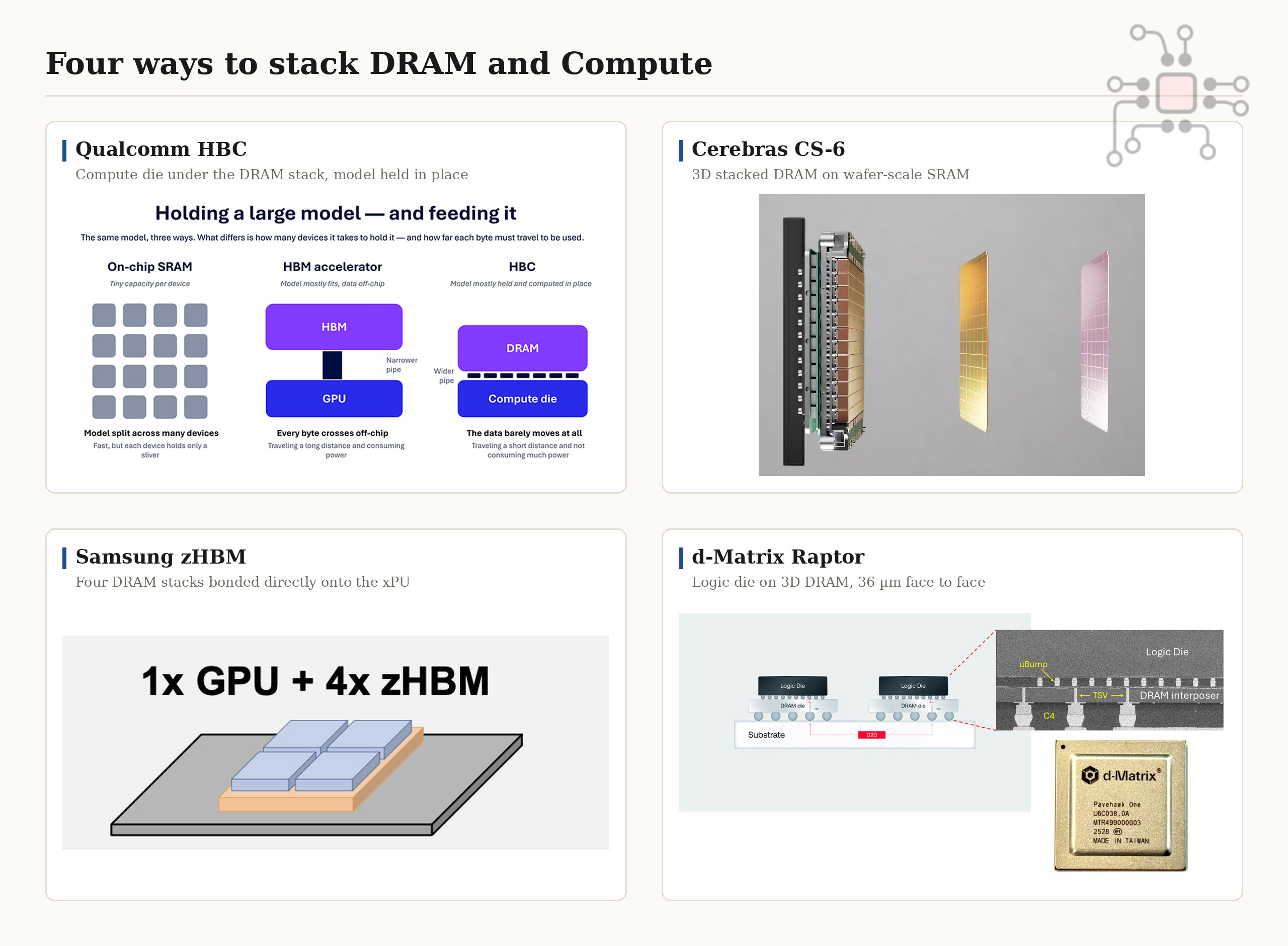
Qualcomm announced HBC (High Bandwidth Compute), then at Hot Chips Cerebras said CS-6 would have a DRAM wafer stacked on top of their compute wafer. Samsung has been relentlessly pumping their zHBM technology, which they call their end goal. There are rumors of Groq LP40 considering stacked DRAM as well. And then d-Matrix presented at depth their second generation accelerator, Raptor, with stacked DRAM, along with a NVIDIA partnership.
In this article I’ll lay out the case for why this trend makes sense. I’ll dig into three specific reasons.
3D DRAM enables the most performant architectures
3D DRAM gives you a path below 0.1 pJ/bit, which frees the power budget for compute and networking
Unlike HBM, 3D DRAM access can be made deterministic like SRAM
3D DRAM enables the best and most performant architectures
The best session at NVIDIA’s GTC this year was the fireside chat between two GOATs, Bill Dally (Chief Scientist at NVIDIA), and Jeff Dean (ex-Chief Scientist at Google DeepMind). Between them they are responsible for a good chunk of modern computing. Of all the things they covered, there was just one idea they kept coming back to —the most energy efficient and performant way to handle computations is to keep the data right next to the tensor engines, and try not to move it.
Typically doing a multiply-add for NVFP4 is 10 femto-joules, and to pull those 4 bits in from HBM4 at 3-4 pJ/bit that about 15 pico-joules. That’s a 1000X more energy to read one NVFP4 number from external memory that it is to do multiply-and-add. But reading an SRAM is also about 10 fJ. The key thing you can do to reduce energy is don’t move data.
This is essentially the architectural philosophy behind accelerators from Groq, Cerebras, and d-Matrix, where SRAM is co-located with the compute units. But, while SRAM is clearly superior on bandwidth, latency, and on energy per bit, it just runs out of capacity quickly. 3D DRAM is the only way to take the next leap, preserving SRAM-like bandwidth while increasing capacity by an order of magnitude.
Similar to SRAM based architectures, with 3D DRAM every tensor core can get its own chunk of dedicated memory, with dedicated wires to read and write it. That capacity and that bandwidth belong to that tensor core alone, unlike HBM where the memory is usually treated as a unified pool and all the tensor cores sip out of a shared straw.
Jeff Dean described this ideal architecture with stacked DRAM on compute as a pachinko machine. Where you open the gates and the data just tumbles down to its dedicated tensor core.
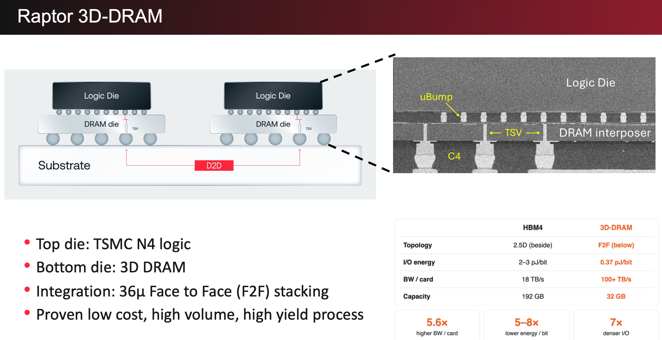
Now, let’s zoom in on d-Matrix's Raptor accelerator, showcased at Hot Chips. It is the first 3D DRAM-based accelerator with a substantial amount of published details.
Package architecture: Each Raptor package has 4 chiplets.
Chiplet design: Each chiplet in this package is a "sandwich" structure consisting of one compute die and one stacked DRAM die.
Compute layout: Each chiplet has 256 tensor engines, and each engine is allocated 3 dedicated DRAM banks, with dedicated wires to read and write them.
Interconnect: Each DRAM bank has a 256 bit bus. That is 196K data lanes between compute and memory on a single chiplet. So each tensor engines has a 768-bit bus it to its dedicated DRAM.
One Raptor Chiplet =
256 Tensor Cores x 3 banks x 256 bit-bus/bank = 196K data lanes

One Raptor Package =
4 chiplets x 196K = ~800K data lates
In comparison, Blackwell package has only 8K data lanes between the GPU and its 8 stacks of HBM3E, and Rubin package has just 16K with 8 stacks of HBM4.
The advantage of an order of magnitude more lanes is that you can run every one of them slowly, around 500-700 MHz, instead of fighting HBM4's 11+ Gbps per pin and the SI/PI and design complexity that comes with it. Running 196K lanes this slowly has another big advantage, which we'll get to in the next section.
As for the numbers,
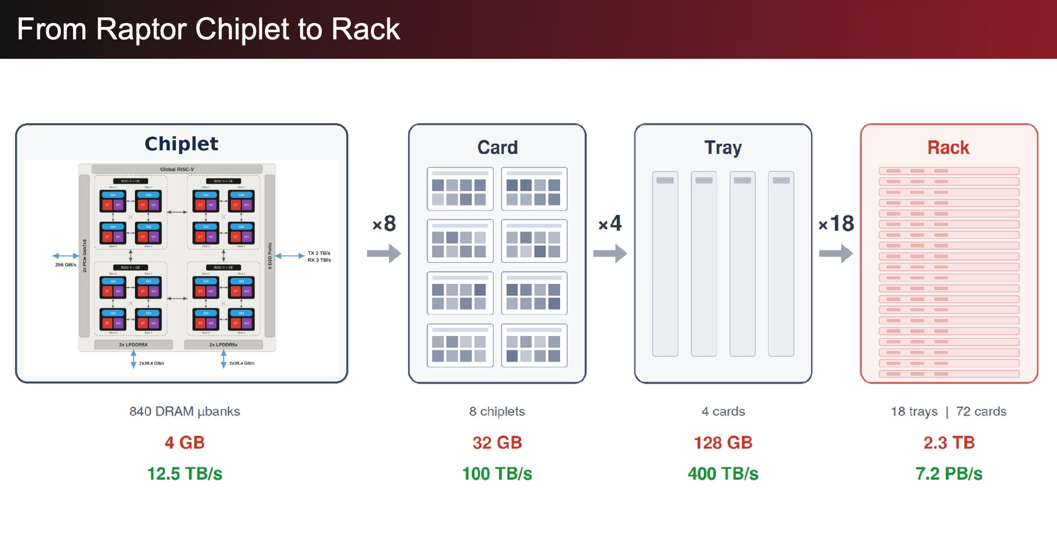
d-Matrix advertises performance per pair of chips (8 chiplets), as shown in the image below. This pair yields 100+ TB/s of memory bandwidth.
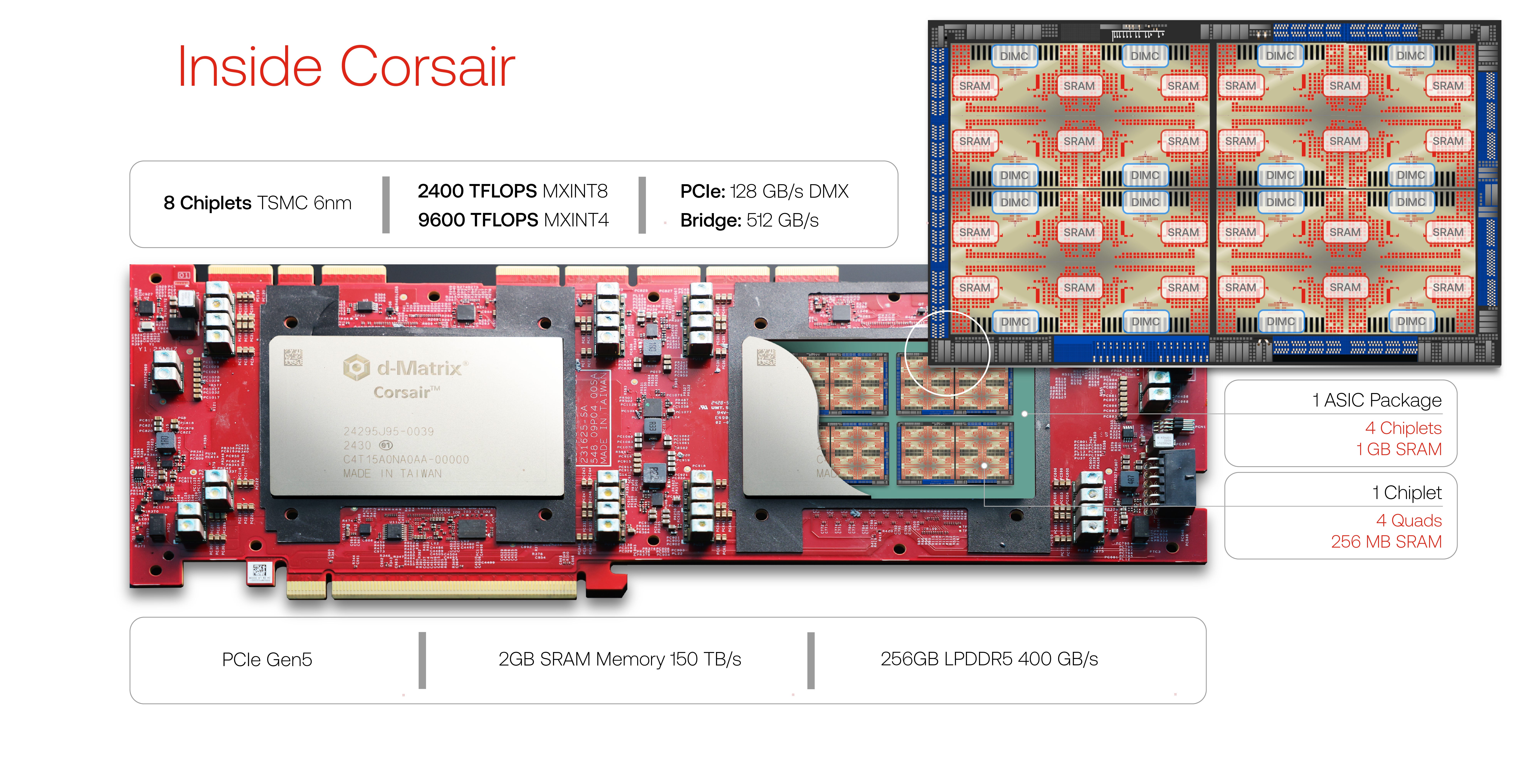
Compared to the 2GB of SRAM in the first-gen Corsair accelerator, Raptor will have 32GB of stacked DRAM.
At the rack level, 18 compute trays, each with 8 raptor packages yield a total 2.3TB of 3D-DRAM with 7.2 PB/s of memory bandwidth. In comparison, an NVL rack with 72 Rubin GPUs does 1.6PB/s of HBM4 bandwidth.
And this is just the first generation of 3D-DRAM based accelerator.
Here's the main takeaway. Several companies have expounded on the benefits of SRAM based inference accelerators. In roadmap terms, 3D DRAM is the only way to take the next leap, preserving SRAM-like bandwidth while increasing capacity.
3D DRAM gets you to < 0.1 pJ/bit
The power angle is actually pretty easy to understand.
In HBM, the energy spent in the DRAM array itself is not the problem. Transporting the data between the memory stack and the compute die through the interposer is. Overcoming all that capacitance requires large drivers and every portion of the path adds to the energy consumption — laterally across the HBM base die to reach the bump, down through the interposer, back up to the compute die's bump, and then laterally once again across the compute die to its destination. Together, those segments cost ~2.5 pJ/bit.
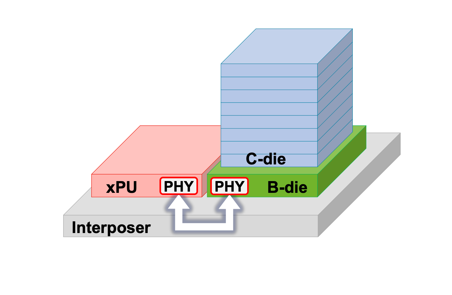
When DRAM is stacked directly on the compute die and it's easy to visualize how little distance the data has to travel between the DRAM bit cell and the point where compute happens. The interposer is eliminated entirely, and that gets us to 0.35-0.4 pJ/bit.
To put 2.5 pJ/bit vs 0.4 pJ/bit in perspective, convert it to watts by multiplying by the bandwidth. Extracting 100 TB/s from a collection of HBM stacks costs 2000W. From 3D DRAM, it costs 296W. Let that sink in for a second. It costs an order of magnitude more power to extract 100 TB/s from HBM than from 3D DRAM. See below to see how these numbers are derived.
HBM power for 100TB/s = 2.5 pJ/bit  x 100 TB/s x 8 bits = 2000W
3DD power for 100TB/s = 0.37 pJ/bit x 100 TB/s x 8 bits = 296W
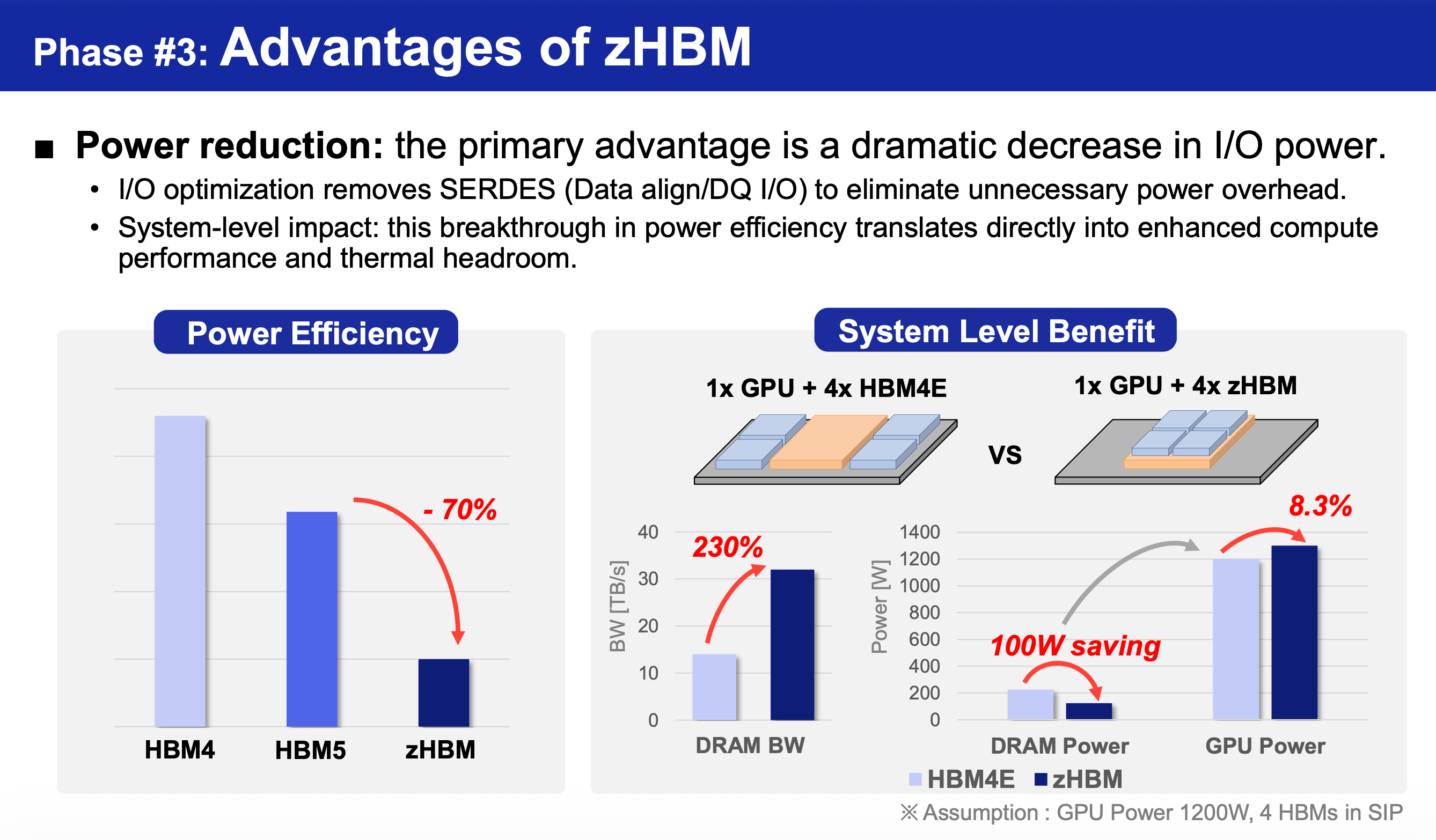
You can even see this in Samsung’s zHBM presentation too. They make a case where in a 1200W GPU system, the savings from zHBM can be diverted towards compute.
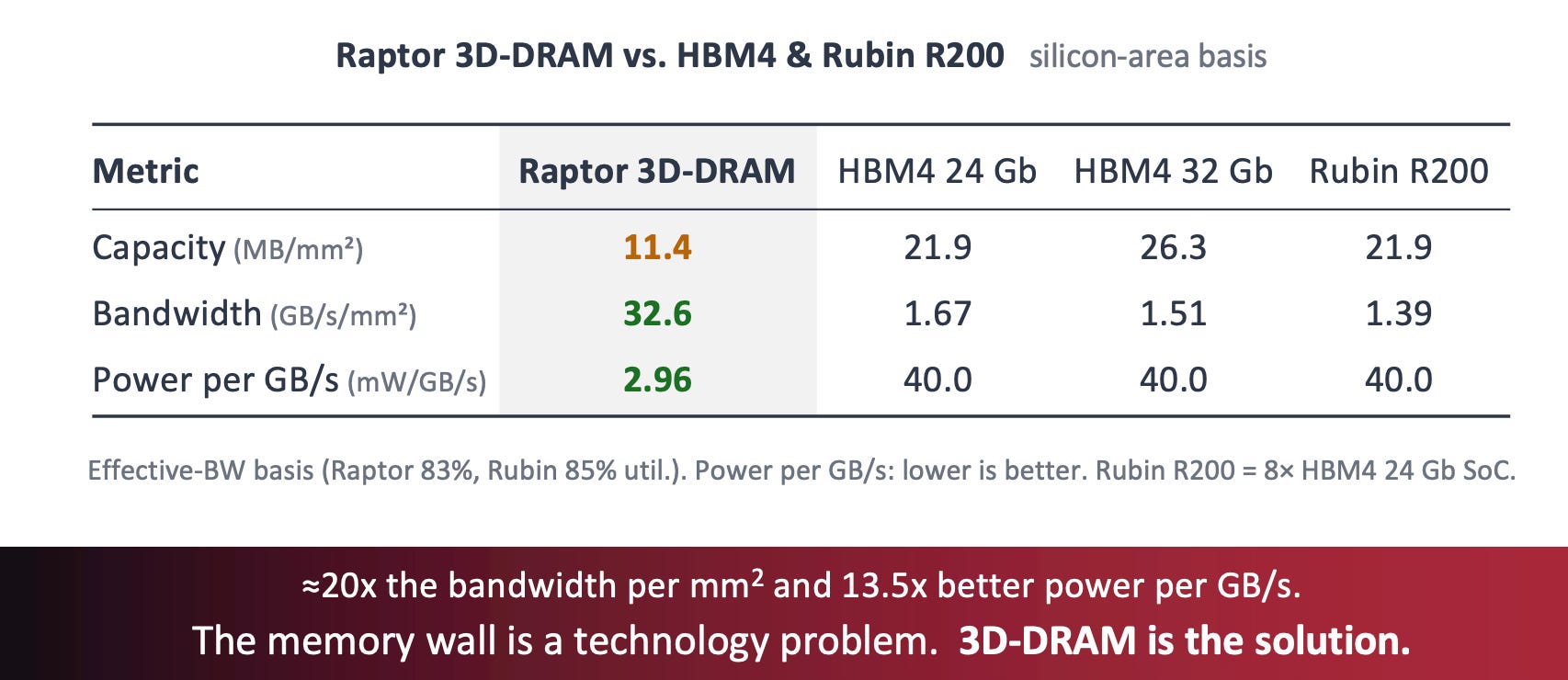
But here’s the thing. 0.37 pJ/bit isn’t the floor.
Raptor bonds its two dies with micro-bumps at a 36 micron pitch. Next to a pad that size, a 4nm transistor driver is tiny, and the pad, its ESD protection, and the routing to reach it form a large capacitor by on-die standards. The same is true on the DRAM side.
Hybrid bonding shrinks all of it. The pitch drops from 36 microns to single-digit microns, the pads shrink with it. The routing distance between the drivers in the compute die and the DRAM is much lesser, and so is the capacitance. So the energy consumed falls even further from ~0.4 pJ/bit to ~0.1 pJ/bit.
3D DRAM access can be made deterministic like SRAM
Ok, the last piece of my sales pitch is this — DRAM is notorious for being non-deterministic.
HBM, LPDDR and similar memories go through a boot-up initialization called training and calibration. This is where the HBM PHY on the compute die runs read centering and write centering algorithms. It writes well-known patterns to the memory, reads them back, and sweeps the phase rotators on each lane to find the center of the data eye. I'm trivializing the process. I've written about the details at length in other posts if you're interested.
Training is only the start. After boot, three things keep DRAM non-deterministic.
Voltage and temperature changes cause that optimal eye to drift, so the PHY has to periodically recalibrate. This is one source of non-determinism.
Refresh is temperature controlled. It’s a required operation, and it takes directly away from performance.
DRAM is very sensitive to how data is stored and retrieved. Since HBM is usually treated as a unified memory, the HBM controller reorders transactions to maximize page hits and bank rotation. That makes the latency of any read request non-deterministic.
With 3D DRAM, these issues either don’t apply or are easy to design around.
When DRAM is bonded directly to compute, the distance is so short you don't need a traditional HBM-style PHY. There's no training and calibration, and no trace lengths to train. The interface between the compute die and the memory die is closed with static timing analysis, which is why this is sometimes called a PHY-less design.
In 3D DRAM, each bank is shallow, so we can set refresh to a high enough rate without taking a big hit to performance.
Each tensor engine has a dedicated path and dedicated pins to its banks, shared with no other tensor engine. So the controller is very simple, and no opportunistic transaction reordering is required. That makes access latency deterministic.
The key takeaway is this. SRAM's deterministic behavior has several big benefits, and 3D DRAM keeps that behavior in a way HBM can't. The one thing to keep in mind is that DRAM as a technology is sensitive to how data is stored and retrieved. Unlike SRAM, where the access pattern doesn't matter, DRAM of any kind, HBM or 3D DRAM, needs some SW/HW co-design so that weights and KV cache are laid out to maximize page hits.
Conclusion
The common questions are about thermals, cooling, warpage, PDN (power delivery network), and yield. These are fair questions and they are solvable. Most of the industry is already working on them. HBM5 is already expected to use hybrid bonding, and the technology is getting ready for prime time.
On thermals, a 4-high stack is probably what we can reach in the immediate future. 8-high still has issues to be engineered through. The real problem is the power density of the compute die sitting underneath the memory stack. DRAM hates heat, and at 0.5 W/mm², getting to 4-high may not be a problem. A GPU like Rubin, at 1.5 W/mm², might get to 2-high easily and might need some engineering to get to 4-high.
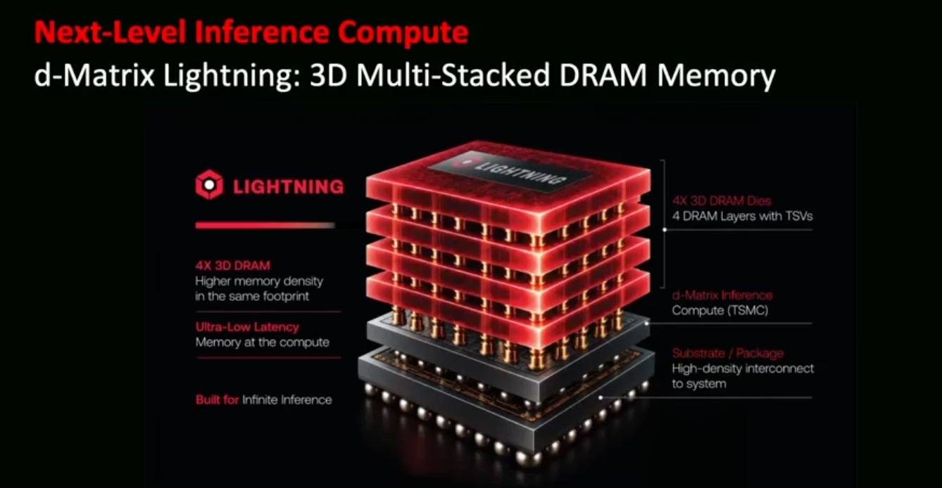
These comments are based on my experience and intuition. The larger point I'm trying to make is this. There's a reason Raptor has one layer of DRAM, and Lightning, the accelerator after it, will have four. There's engineering to be figured out beyond that.
That’s it for this session. Please do share this article and subscribe to Chiplog if you found it useful. Cheers!
Disclosure: I work at d-Matrix and was part of the 3D-DRAM subsystem implementation described here. Take the enthusiasm with the appropriate grain of salt.