


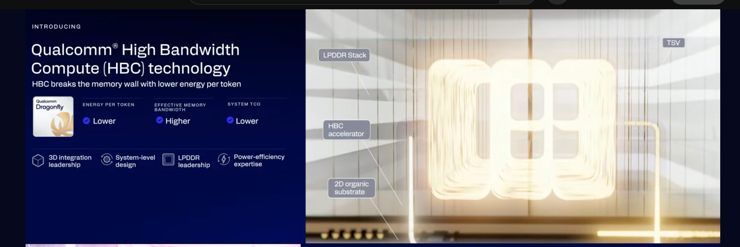
At Qualcomm’s Investor Day 2026, the company laid out a genuinely exciting roadmap for its AI silicon. But the most interesting part, High Bandwidth Compute (HBC), and the near-memory compute that goes with it, came with remarkably slim details.
In this short post:
I’ll speculate on who the memory vendor behind the stack could be, and explain why I think the “LPDDR” label on Qualcomm’s slides is a slight red herring.
I’ll lay out the questions we should be asking about the XPU die sitting under the memory.
I’ll argue that the mid-2027 date for AI250 is unlikely to hold, with a slip to late 2027 or early 2028 looking more realistic.

3D Stacked Memory
Stacking DRAM directly on compute is quickly becoming the industry’s default answer to the memory wall. d-Matrix is pursuing it, Cerebras is reportedly exploring it, and SemiAnalysis has reported that even NVIDIA will use hybrid-bonded DRAM to extend on-chip memory in the Groq LP40 chip. So from a general technology trend, Qualcomm’s High Bandwidth Compute (HBC) is exactly the direction you’d expect the company to take.
And it’s the details where HBC gets interesting, because the more you look at what Qualcomm has actually shown, the more the questions pile up.
The LPDDR label is a red herring
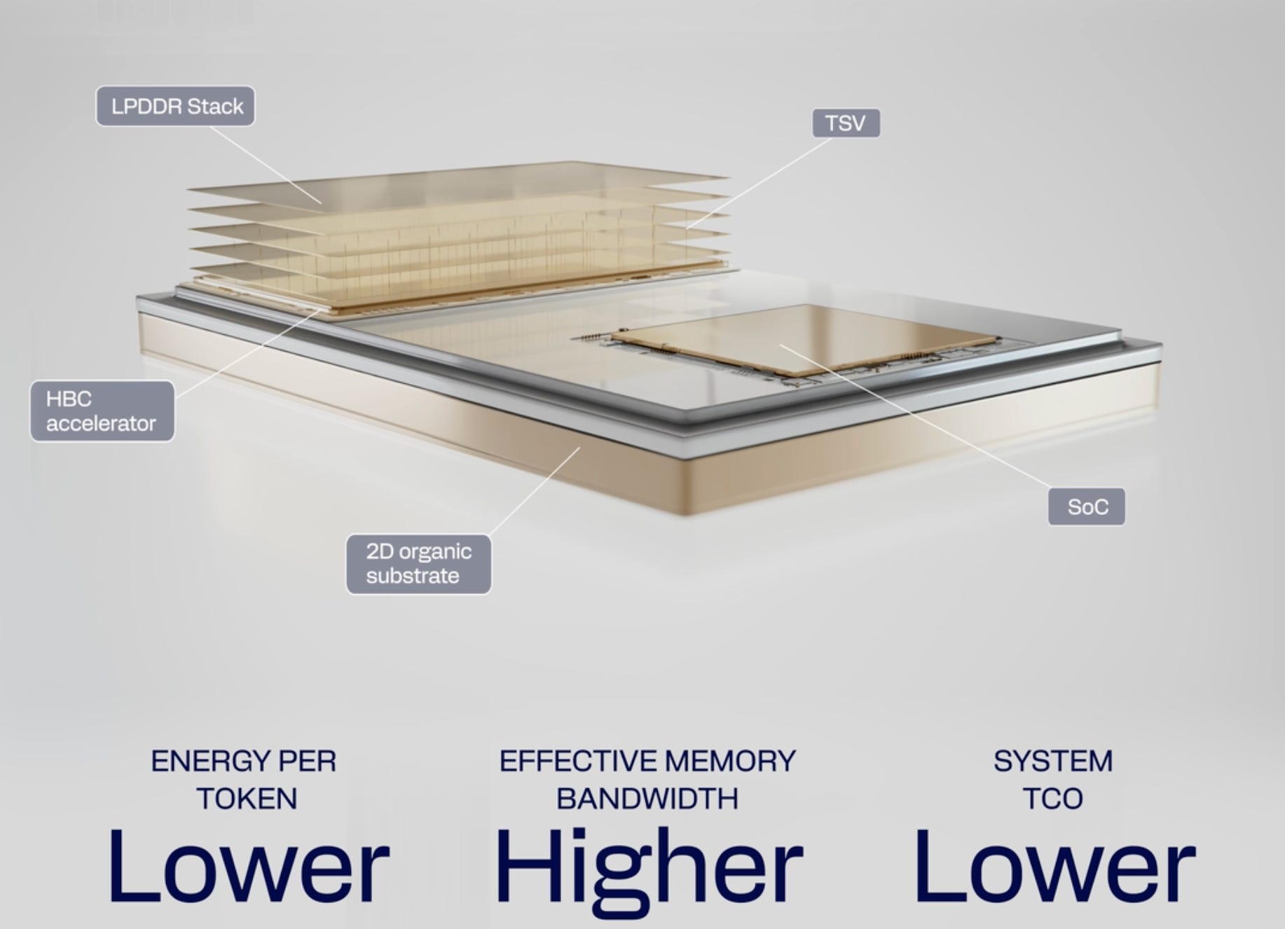
In the Investor Day slides, Qualcomm labels the memory stack “LPDDR.” My hot take: that label is misleading, and there’s nothing truly LPDDR (in the JEDEC sense) about what this is going to be.