

Analysis of NVIDIA DGX Spark's GB10 SoC
Architecture, methodology, and memory interface of the GB10 SoC

This article takes a closer look at the Grace-Blackwell GB10 SoC, the chip powering NVIDIA’s newly released DGX Spark. Here’s a quick timeline of how we got here:
January 2025 : NVIDIA announced Project DIGITS at CES, revealing the form factor, compute capabilities, and a new partnership with MediaTek to co-develop the GB10 chip.
March 2025: The project was officially renamed DGX Spark, replacing the DIGITS codename.
September 2025: Chief Architect of the GB10 SoC, Andi Skende, shared its architecture and development process in great detail at the Hot Chips conference.
October 2025: DGX Spark officially began shipping.
Architecture
2.5D
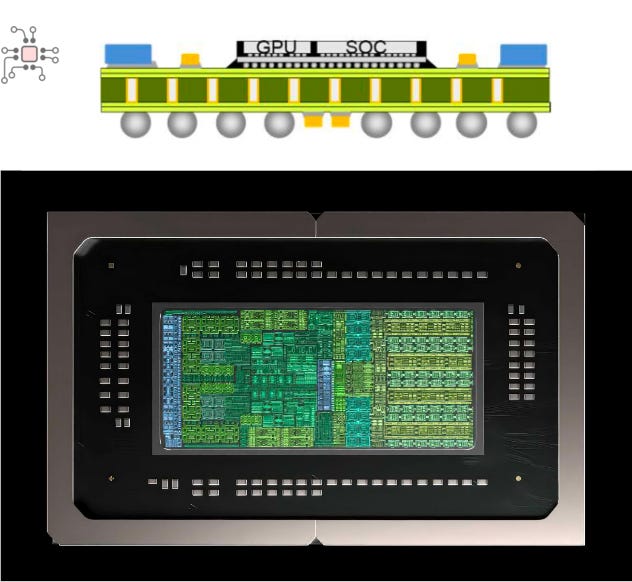
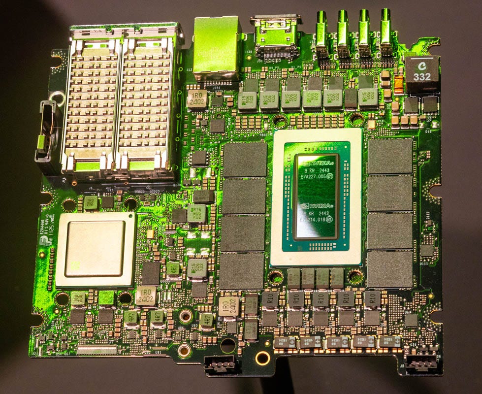
Like other Grace-Hopper (GH) and Grace-Blackwell (GB) configurations, the GB10 has a CPU and a GPU component. However, unlike its higher-end counterparts, the GH200 and GB200, where the CPU and GPU are housed in separate packages, the GB10 uses a multi-die package. In this design, the CPU and GPU dies are connected via C2C interconnect over an interposer, following a 2.5D integration approach.
Not really the Grace CPU
In my opinion, this was the biggest surprise. Although the CPU is labeled “Grace,” it’s not a cut-down version of the Grace CPU used in GH200, GB200, or the Grace Superchip systems. Instead, it’s a 20-Core ARM CPU IP developed by MediaTek.
While NVIDIA had announced its partnership with MediaTek back in January, I did not expect such a deep collaboration. This isn’t a small integration, it’s a full-fledged co-design effort.
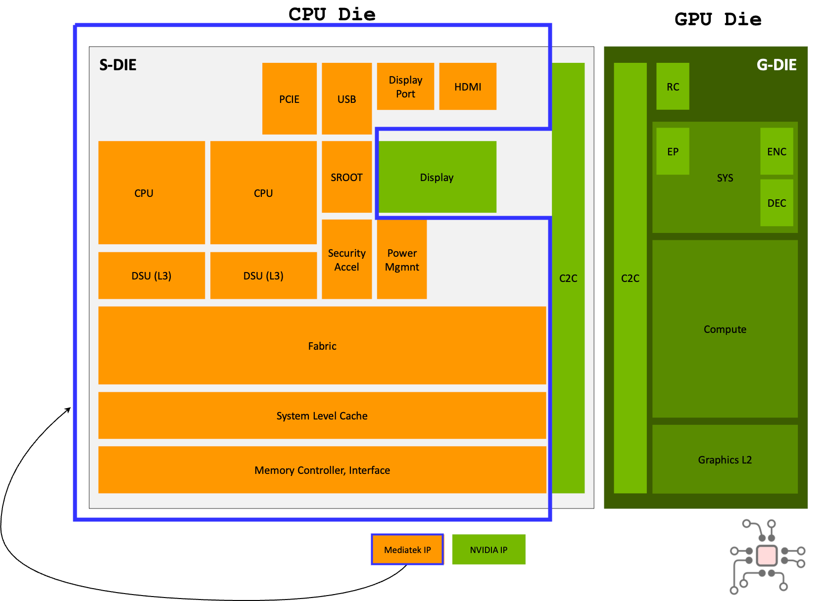
Memory subsystem
The Blackwell iGPU die, as expected, is based on NVIDIA’s Blackwell GPU architecture. It doesn’t have dedicated memory of its own. Instead, it connects to the system’s LPDDR5X DRAM through memory controllers located in the MediaTek CPU die. The C2C interconnect provides around 600 GB/s of aggregate bandwidth, more than enough for the iGPU to access the full system memory bandwidth.
This kind of data flow, where the GPU accesses memory attached to the CPU in a unified fashion, isn’t new. It’s an approach we saw in Grace Hopper presentations, and the DGX Spark simply extends that same design philosophy.
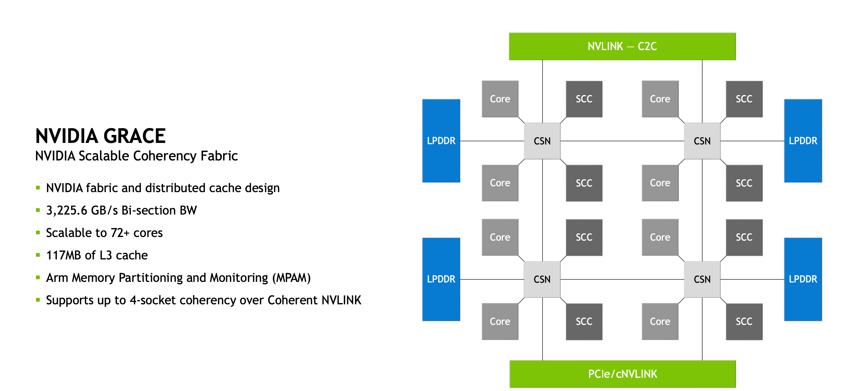
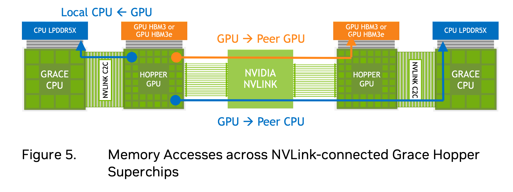
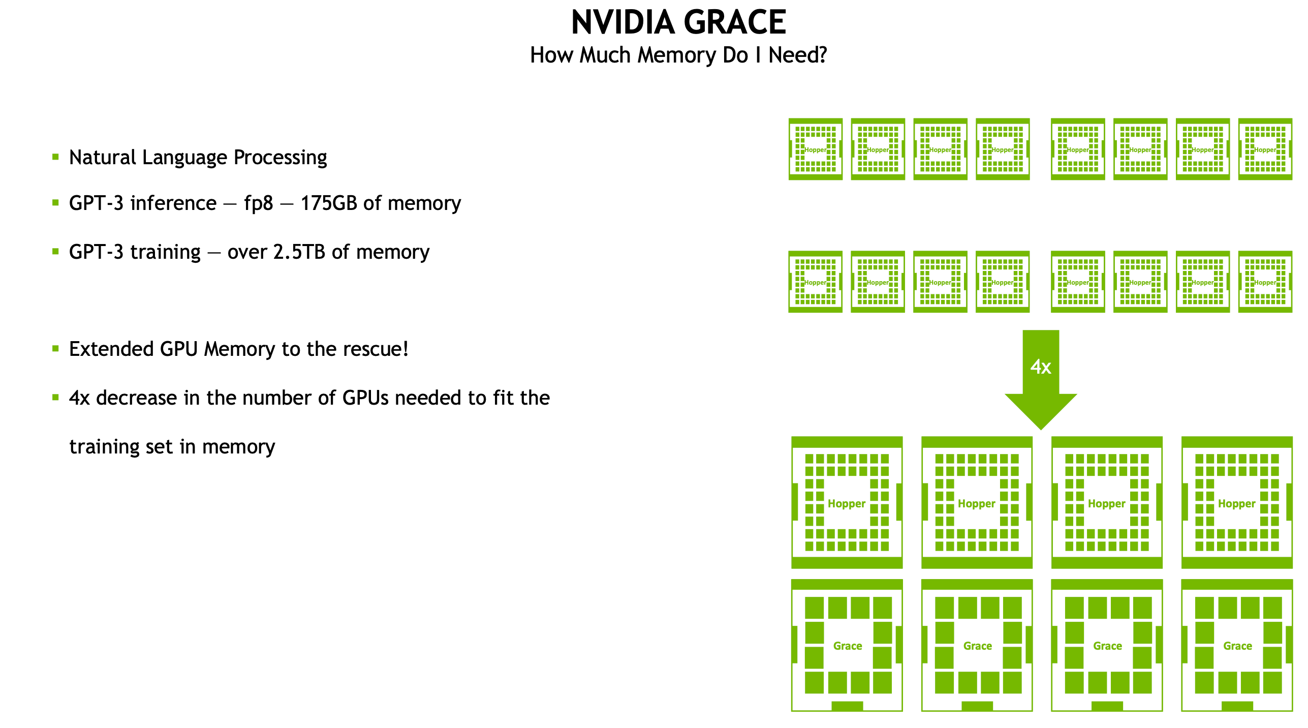
Here are 2 slides from the Grace CPU and Grace Hopper architecture document, where this unified memory model is emphasized.
The GPU can access LPDDR5X memory over NVLink C2C in a coherent and transparent manner.
It’s more efficient to have 4× Grace + 4× Hopper nodes rather than 16× Hopper, to reach the 2.5 TB memory footprint required for training.
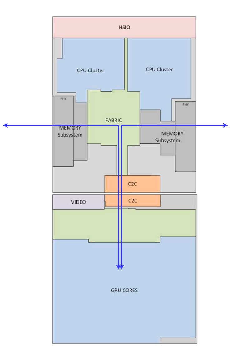
GB10 Memory Complex
Regarding the memory subsystem itself:
The memory controllers are part of the MediaTek CPU IP.
There are 8 LPDDR5X DRAM packages soldered to the board, each with a 32-bit interface, for a total interface width of 256 bits.
The datasheet lists total memory bandwidth at 273 GB/s, which corresponds to a memory speed of 8.533 Gbps.
(256 bits × 8.533 Gbps)/8 = 273 GB/sIn the Hot Chips presentation, the memory clock was specified as 9.4 Gbps (300 GB/s of bandwidth). Suggesting some capability to overclock, perhaps?
Methodology
In his Hot Chips presentation, Andi Skende, GB10’s chief architect, spent considerable time detailing the verification strategies used in developing the chip.
Here are few excerpts from the talk, with my comments in italics:
We had to do very extensive performance modeling of the GPU IP traffic into MediaTek’s memory controller subsystem to make sure we achieve the best efficiency while also giving the CPU core reasonable latency. It is a challenging problem to balance UMA (Unified Memory Access) architecture where latency and efficiency are competing with each other.
We followed a very strict IP model when delivering our IP to MediaTek for integration into their SoC, IP such as the C2C and Display. (NVIDIA sent over their IPs to MediaTek. So, MediaTek closed timing, did synthesis, and all backend work for the CPU die?)
On the verification side, we took a multi-prong approach, we used BFMs (Bus Functional Models) where possible and a hierarchical approach to verification.
We did co-simulation for very complex features that required end-to-end simulation by bringing the 2 dies together into a co-simulation platform. CPU to GPU coherency is one such feature that requires a lot of verification and co-simulation to make sure you’ve covered all the corner cases, there are no race conditions, no deadlocks, etc.
Last but not the least we relied on emulation very heavily, to bring together MediaTek’s hardware, NVIDIA hardware, firmware and software, working together pre-silicon. Where we booted the whole OS including running full app frames before we taped-out, and all that enabled us to tape-out and go to production with first silicon, A0 silicon, one tape-out no respins.
Andi Skende, Hot Chips 2025
Chiplog Note: Simulation and emulation are pre-silicon verification strategies. Simulation can only be done on smaller portions of the design and aperture of time for which the design can be checked is small, in the order of milliseconds.
In emulation, larger portions of the design are synthesized and run on dedicated hardware like Cadence’s Palladium or Siemens Mentor Graphics’ Veloce. The hardware and licenses for emulation itself cost millions of dollars.
Executing collaborations of this scale and shipping A0 silicon is an admirable achievement, even for a company like NVIDIA with virtually unlimited resources.
Conclusion
As expected, there’s been plenty of discussion in forums and comment sections about whether the DGX Spark justifies its $4,000 price tag, and how it stacks up against the RTX 5090 or an equivalently configured Apple Mac Studio. But regardless of raw performance metrics, this project is a major win for NVIDIA.
Designing this chip entirely in-house would have required a dedicated team and measurably more engineering resources, likely pulling focus away from NVIDIA’s main high-end SoC efforts. Instead, by co-designing with MediaTek, leveraging their CPU and memory controller IPs, and establishing a collaborative workflow that lead to a successful A0 tape-out is a significant feather in NVIDIA’s cap.
NVIDIA can now pursue the DGX Spark product line and build successors to the GB10 with lesser internal overhead.
Support Chiplog
Chiplog is a reader-support publication. To receive new posts and support my work, consider becoming a free or paid subscriber.
Right now memberships are 50% off. That’s $37.5/year (~$3/month).